JAJSQH4
october 2020
BQ25302
PRODUCTION DATA
1
1
特長
2
アプリケーション
3
概要
4
Revision History
5
概要 (続き)
6
Pin Configuration and Functions
7
Specifications
7.1
Absolute Maximum Ratings
7.2
ESD Ratings
7.3
Recommended Operating Conditions
7.4
Thermal Information
7.5
Electrical Characteristics
7.6
Timing Requirements
7.7
Typical Characteristics
8
Detailed Description
8.1
Overview
8.2
Functional Block Diagram
8.3
Feature Description
8.3.1
Device Power Up
8.3.1.1
Power-On-Reset (POR)
8.3.1.2
REGN Regulator Power Up
8.3.1.3
Charger Power Up
8.3.1.4
Charger Enable and Disable by EN Pin
8.3.1.5
Device Unplugged from Input Source
8.3.2
Battery Charging Management
8.3.2.1
Battery Charging Profile
8.3.2.2
Precharge
8.3.2.3
Charging Termination
8.3.2.4
Battery Recharge
8.3.2.5
Charging Safety Timer
8.3.2.6
Thermistor Temperature Monitoring
8.3.3
Charging Status Indicator (STAT)
8.3.4
Protections
8.3.4.1
Voltage and Current Monitoring
8.3.4.1.1
Input Over-Voltage Protection
8.3.4.1.2
Input Voltage Dynamic Power Management (VINDPM)
8.3.4.1.3
Input Current Limit
8.3.4.1.4
Cycle-by-Cycle Current Limit
8.3.4.2
Thermal Regulation and Thermal Shutdown
8.3.4.3
Battery Protection
8.3.4.3.1
Battery Over-Voltage Protection (VBAT_OVP)
8.3.4.3.2
Battery Short Circuit Protection
8.3.4.4
ICHG Pin Open and Short Protection
8.4
Device Functional Modes
8.4.1
Disable Mode, HiZ Mode, Sleep Mode, Charge Mode, Termination Mode, and Fault Mode
9
Application and Implementation
9.1
Application Information
9.2
Typical Applications
9.2.1
Typical Application
9.2.1.1
Design Requirements
9.2.1.2
Detailed Design Procedure
9.2.1.2.1
Charge Voltage Settings
9.2.1.2.2
Charge Current Setting
9.2.1.2.3
Inductor Selection
9.2.1.2.4
Input Capacitor
9.2.1.2.5
Output Capacitor
9.2.1.3
Application Curves
9.2.2
Typical Application with External Power Path
9.2.2.1
Design Requirements
9.2.3
Typical Application with MCU Programmable Charge Current
9.2.3.1
Design Requirements
10
Power Supply Recommendations
11
Layout
11.1
Layout Guidelines
11.2
Layout Example
12
デバイスおよびドキュメントのサポート
12.1
デバイスのサポート
12.1.1
サード・パーティ製品に関する免責事項
12.2
ドキュメントのサポート
12.2.1
関連資料
12.3
ドキュメントの更新通知を受け取る方法
12.4
サポート・リソース
12.5
Trademarks
12.6
静電気放電に関する注意事項
12.7
用語集
13
Mechanical, Packaging, and Orderable Information
パッケージ・オプション
メカニカル・データ(パッケージ|ピン)
RTE|16
MPQF149D
サーマルパッド・メカニカル・データ
RTE|16
QFND525B
発注情報
jajsqh4_oa
jajsqh4_pm
7.7
Typical Characteristics
f
SW
= 1.2 MHz
Inductance 1 uH
V
BUS
= 5 V
Inductor DCR = 14.6 mΩ
Figure 7-1
Battery Charge Efficiency vs. Charge Current
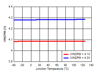
Figure 7-3
VINDPM vs. Junction Temperature
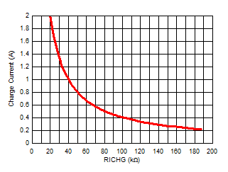
Figure 7-5
Charge Current vs. Charge Current Setting Resistance RICHG
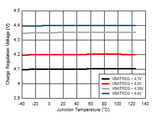
Figure 7-2
Battery Charge Regulation Voltage vs. Junction Temperature
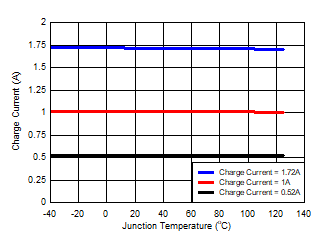
Figure 7-4
Charge Current vs. Junction Temperature
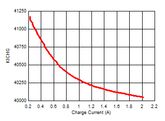
Figure 7-6
KICHG vs. Charge Current