JAJSQH4 october   2020 BQ25302

PRODUCTION DATA  

  1.   1
  2. 特長
  3. アプリケーション
  4. 概要
  5. Revision History
  6. 概要 (続き)
  7. Pin Configuration and Functions
  8. Specifications
    1. 7.1 Absolute Maximum Ratings
    2. 7.2 ESD Ratings
    3. 7.3 Recommended Operating Conditions
    4. 7.4 Thermal Information
    5. 7.5 Electrical Characteristics
    6. 7.6 Timing Requirements
    7. 7.7 Typical Characteristics
  9. Detailed Description
    1. 8.1 Overview
    2. 8.2 Functional Block Diagram
    3. 8.3 Feature Description
      1. 8.3.1 Device Power Up
        1. 8.3.1.1 Power-On-Reset (POR)
        2. 8.3.1.2 REGN Regulator Power Up
        3. 8.3.1.3 Charger Power Up
        4. 8.3.1.4 Charger Enable and Disable by EN Pin
        5. 8.3.1.5 Device Unplugged from Input Source
      2. 8.3.2 Battery Charging Management
        1. 8.3.2.1 Battery Charging Profile
        2. 8.3.2.2 Precharge
        3. 8.3.2.3 Charging Termination
        4. 8.3.2.4 Battery Recharge
        5. 8.3.2.5 Charging Safety Timer
        6. 8.3.2.6 Thermistor Temperature Monitoring
      3. 8.3.3 Charging Status Indicator (STAT)
      4. 8.3.4 Protections
        1. 8.3.4.1 Voltage and Current Monitoring
          1. 8.3.4.1.1 Input Over-Voltage Protection
          2. 8.3.4.1.2 Input Voltage Dynamic Power Management (VINDPM)
          3. 8.3.4.1.3 Input Current Limit
          4. 8.3.4.1.4 Cycle-by-Cycle Current Limit
        2. 8.3.4.2 Thermal Regulation and Thermal Shutdown
        3. 8.3.4.3 Battery Protection
          1. 8.3.4.3.1 Battery Over-Voltage Protection (VBAT_OVP)
          2. 8.3.4.3.2 Battery Short Circuit Protection
        4. 8.3.4.4 ICHG Pin Open and Short Protection
    4. 8.4 Device Functional Modes
      1. 8.4.1 Disable Mode, HiZ Mode, Sleep Mode, Charge Mode, Termination Mode, and Fault Mode
  10. Application and Implementation
    1. 9.1 Application Information
    2. 9.2 Typical Applications
      1. 9.2.1 Typical Application
        1. 9.2.1.1 Design Requirements
        2. 9.2.1.2 Detailed Design Procedure
          1. 9.2.1.2.1 Charge Voltage Settings
          2. 9.2.1.2.2 Charge Current Setting
          3. 9.2.1.2.3 Inductor Selection
          4. 9.2.1.2.4 Input Capacitor
          5. 9.2.1.2.5 Output Capacitor
        3. 9.2.1.3 Application Curves
      2. 9.2.2 Typical Application with External Power Path
        1. 9.2.2.1 Design Requirements
      3. 9.2.3 Typical Application with MCU Programmable Charge Current
        1. 9.2.3.1 Design Requirements
  11. 10Power Supply Recommendations
  12. 11Layout
    1. 11.1 Layout Guidelines
    2. 11.2 Layout Example
  13. 12デバイスおよびドキュメントのサポート
    1. 12.1 デバイスのサポート
      1. 12.1.1 サード・パーティ製品に関する免責事項
    2. 12.2 ドキュメントのサポート
      1. 12.2.1 関連資料
    3. 12.3 ドキュメントの更新通知を受け取る方法
    4. 12.4 サポート・リソース
    5. 12.5 Trademarks
    6. 12.6 静電気放電に関する注意事項
    7. 12.7 用語集
  14. 13Mechanical, Packaging, and Orderable Information

パッケージ・オプション

メカニカル・データ(パッケージ|ピン)
サーマルパッド・メカニカル・データ
発注情報

Typical Application with External Power Path

In the case where a system needs to be immediately powered up from VBUS when the battery is overdischarged or dead, the application circuit shown in Figure 9-6 can be used to provide a power path from VBUS/PMID to VSYS. PFET Q4 is an external PFET that turns on to supply VSYS from the battery when VBUS is removed; PFET Q4 turns off when VBUS is plugged in and VSYS is supplied from VBUS/PMID.
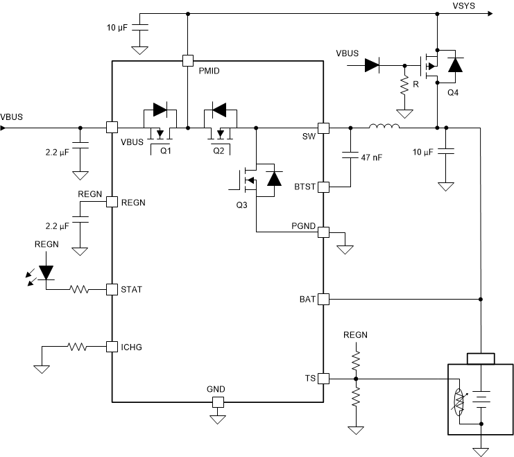
GUID-20201014-CA0I-6JG9-LX08-6FBTQDS2D5WC-low.gif Figure 9-6 Typical Application Diagram with Power Path