JAJSD78A
May 2017 – May 2018
PRODUCTION DATA.
1
特長
2
アプリケーション
3
概要
Device Images
アプリケーション図
4
改訂履歴
5
概要(続き)
6
Pin Configuration and Functions
Pin Functions
7
Specifications
7.1
Absolute Maximum Ratings
7.2
ESD Ratings
7.3
Recommended Operating Conditions
7.4
Thermal Information
7.5
Electrical Characteristics
7.6
Timing Requirements
7.7
Typical Characteristics
8
Detailed Description
8.1
Overview
8.2
Functional Block Diagram
8.3
Feature Description
8.3.1
Power-Up from Battery Without DC Source
8.3.2
Power-Up From DC Source
8.3.2.1
CHRG_OK Indicator
8.3.2.2
Input Voltage and Current Limit Setup
8.3.2.3
Battery Cell Configuration
8.3.2.4
Device Hi-Z State
8.3.3
USB On-The-Go (OTG)
8.3.4
Converter Operation
8.3.4.1
Inductor Setting through IADPT Pin
8.3.4.2
Continuous Conduction Mode (CCM)
8.3.4.3
Pulse Frequency Modulation (PFM)
8.3.5
Current and Power Monitor
8.3.5.1
High-Accuracy Current Sense Amplifier (IADPT and IBAT)
8.3.5.2
High-Accuracy Power Sense Amplifier (PSYS)
8.3.6
Input Source Dynamic Power Manage
8.3.7
Two-Level Adapter Current Limit (Peak Power Mode)
8.3.8
Processor Hot Indication
8.3.8.1
PROCHOT During Low Power Mode
8.3.8.2
PROCHOT Status
8.3.9
Device Protection
8.3.9.1
Watchdog Timer
8.3.9.2
Input Overvoltage Protection (ACOV)
8.3.9.3
Input Overcurrent Protection (ACOC)
8.3.9.4
System Overvoltage Protection (SYSOVP)
8.3.9.5
Battery Overvoltage Protection (BATOVP)
8.3.9.6
Battery Short
8.3.9.7
Thermal Shutdown (TSHUT)
8.4
Device Functional Modes
8.4.1
Forward Mode
8.4.1.1
System Voltage Regulation with Narrow VDC Architecture
8.4.1.2
Battery Charging
8.4.2
USB On-The-Go
8.5
Programming
8.5.1
I2C Serial Interface
8.5.1.1
Data Validity
8.5.1.2
START and STOP Conditions
8.5.1.3
Byte Format
8.5.1.4
Acknowledge (ACK) and Not Acknowledge (NACK)
8.5.1.5
Slave Address and Data Direction Bit
8.5.1.6
Single Read and Write
8.5.1.7
Multi-Read and Multi-Write
8.5.1.8
Write 2-Byte I2C Commands
8.6
Register Map
8.6.1
Setting Charge and PROCHOT Options
8.6.1.1
ChargeOption0 Register (I2C address = 01/00h) [reset = E20Eh]
Table 5.
ChargeOption0 Register (I2C address = 01h) Field Descriptions
Table 6.
ChargeOption0 Register (I2C address = 00h) Field Descriptions
8.6.1.2
ChargeOption1 Register (I2C address = 31/30h) [reset = 211h]
Table 7.
ChargeOption1 Register (I2C address = 31h) Field Descriptions
Table 8.
ChargeOption1 Register (I2C address = 30h) Field Descriptions
8.6.1.3
ChargeOption2 Register (I2C address = 33/32h) [reset = 2B7]
Table 9.
ChargeOption2 Register (I2C address = 33h) Field Descriptions
Table 10.
ChargeOption2 Register (I2C address = 32h) Field Descriptions
8.6.1.4
ChargeOption3 Register (I2C address = 35/34h) [reset = 0h]
Table 11.
ChargeOption3 Register (I2C address = 35h) Field Descriptions
Table 12.
ChargeOption3 Register (I2C address = 34h) Field Descriptions
8.6.1.5
ProchotOption0 Register (I2C address = 37/36h) [reset = 04A54h]
Table 13.
ProchotOption0 Register (I2C address = 37h) Field Descriptions
Table 14.
ProchotOption0 Register (I2C address = 36h) Field Descriptions
8.6.1.6
ProchotOption1 Register (I2C address = 39/38h) [reset = 8120h]
Table 15.
ProchotOption1 Register (I2C address = 39h) Field Descriptions
Table 16.
ProchotOption1 Register (I2C address = 38h) Field Descriptions
8.6.1.7
ADCOption Register (I2C address = 3B/3Ah) [reset = 2000h]
Table 17.
ADCOption Register (I2C address = 3Bh) Field Descriptions
Table 18.
ADCOption Register (I2C address = 3Ah) Field Descriptions
8.6.2
Charge and PROCHOT Status
8.6.2.1
ChargerStatus Register (I2C address = 21/20h) [reset = 0000h]
Table 19.
ChargerStatus Register (I2C address = 21h) Field Descriptions
Table 20.
ChargerStatus Register (I2C address = 20h) Field Descriptions
8.6.2.2
ProchotStatus Register (I2C address = 23/22h) [reset = 0h]
Table 21.
ProchotStatus Register (I2C address = 23h) Field Descriptions
Table 22.
ProchotStatus Register (I2C address = 22h) Field Descriptions
8.6.3
ChargeCurrent Register (I2C address = 03/02h) [reset = 0h]
Table 23.
Charge Current Register (14h) With 10-mΩ Sense Resistor (I2C address = 03h) Field Descriptions
Table 24.
Charge Current Register (14h) With 10-mΩ Sense Resistor (I2C address = 02h) Field Descriptions
8.6.3.1
Battery Pre-Charge Current Clamp
8.6.4
MaxChargeVoltage Register (I2C address = 05/04h) [reset value based on CELL_BATPRESZ pin setting]
Table 25.
MaxChargeVoltage Register (I2C address = 05h) Field Descriptions
Table 26.
MaxChargeVoltage Register (I2C address = 04h) Field Descriptions
8.6.5
MinSystemVoltage Register (I2C address = 0D/0Ch) [reset value based on CELL_BATPRESZ pin setting]
Table 27.
MinSystemVoltage Register (I2C address = 0Dh) Field Descriptions
Table 28.
MinSystemVoltage Register (I2C address = 0Ch) Field Descriptions
8.6.5.1
System Voltage Regulation
8.6.6
Input Current and Input Voltage Registers for Dynamic Power Management
8.6.6.1
Input Current Registers
8.6.6.1.1
IIN_HOST Register With 10-mΩ Sense Resistor (I2C address = 0F/0Eh) [reset = 4000h]
Table 29.
IIN_HOST Register With 10-mΩ Sense Resistor (I2C address = 0Fh) Field Descriptions
Table 30.
IIN_HOST Register With 10-mΩ Sense Resistor (I2C address = 0Eh) Field Descriptions
8.6.6.1.2
IIN_DPM Register With 10-mΩ Sense Resistor (I2C address = 25/24h) [reset = 0h]
Table 31.
IIN_DPM Register With 10-mΩ Sense Resistor (I2C address = 25h) Field Descriptions
Table 32.
IIN_DPM Register With 10-mΩ Sense Resistor (I2C address = 24h) Field Descriptions
8.6.6.1.3
InputVoltage Register (I2C address = 0B/0Ah) [reset = VBUS-1.28V]
Table 33.
InputVoltage Register (I2C address = 0Bh) Field Descriptions
Table 34.
InputVoltage Register (I2C address = 0Ah) Field Descriptions
8.6.7
OTGVoltage Register (I2C address = 07/06h) [reset = 0h]
Table 35.
OTGVoltage Register (I2C address = 07h) Field Descriptions
Table 36.
OTGVoltage Register (I2C address = 06h) Field Descriptions
8.6.8
OTGCurrent Register (I2C address = 09/08h) [reset = 0h]
Table 37.
OTGCurrent Register (I2C address = 09h) Field Descriptions
Table 38.
OTGCurrent Register (I2C address = 08h) Field Descriptions
8.6.9
ADCVBUS/PSYS Register (I2C address = 27/26h)
Table 39.
ADCVBUS/PSYS Register (I2C address = 27h) Field Descriptions
Table 40.
ADCVBUS/PSYS Register (I2C address = 26h) Field Descriptions
8.6.10
ADCIBAT Register (I2C address = 29/28h)
Table 41.
ADCIBAT Register (I2C address = 29h) Field Descriptions
Table 42.
ADCIBAT Register (I2C address = 28h) Field Descriptions
8.6.11
ADCIINCMPIN Register (I2C address = 2B/2Ah)
Table 43.
ADCIINCMPIN Register (I2C address = 2Bh) Field Descriptions
Table 44.
ADCIINCMPIN Register (I2C address = 2Ah) Field Descriptions
8.6.12
ADCVSYSVBAT Register (I2C address = 2D/2Ch)
Table 45.
ADCVSYSVBAT Register (I2C address = 2Dh) Field Descriptions
Table 46.
ADCVSYSVBAT Register (I2C address = 2Ch) Field Descriptions
8.6.13
ID Registers
8.6.13.1
ManufactureID Register (I2C address = 2Eh) [reset = 0040h]
Table 47.
ManufactureID Register Field Descriptions
8.6.13.2
Device ID (DeviceAddress) Register (I2C address = 2Fh) [reset = 0h]
Table 48.
Device ID (DeviceAddress) Register Field Descriptions
9
Application and Implementation
9.1
Application Information
9.2
Typical Application
9.2.1
Design Requirements
9.2.2
Detailed Design Procedure
9.2.2.1
ACP-ACN Input Filter
9.2.2.2
Inductor Selection
9.2.2.3
Input Capacitor
9.2.2.4
Output Capacitor
9.2.2.5
Power MOSFETs Selection
9.2.3
Application Curves
10
Power Supply Recommendations
11
Layout
11.1
Layout Guidelines
11.2
Layout Example
11.2.1
Layout Consideration of Current Path
11.2.2
Layout Consideration of Short Circuit Protection
12
デバイスおよびドキュメントのサポート
12.1
デバイス・サポート
12.1.1
デベロッパー・ネットワークの製品に関する免責事項
12.2
ドキュメントのサポート
12.2.1
関連資料
12.3
ドキュメントの更新通知を受け取る方法
12.4
コミュニティ・リソース
12.5
商標
12.6
静電気放電に関する注意事項
12.7
Glossary
13
メカニカル、パッケージ、および注文情報
13.1
Package Option Addendum
13.1.1
Packaging Information
13.1.2
Tape and Reel Information
パッケージ・オプション
メカニカル・データ(パッケージ|ピン)
RSN|32
MPQF194B
サーマルパッド・メカニカル・データ
RSN|32
QFND189E
発注情報
jajsd78a_oa
jajsd78a_pm
11.2.2
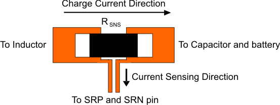
Layout Consideration of Short Circuit Protection
Figure 66.
Sensing Resistor PCB Layout