JAJSVD8 August   2024 BQ25758A

PRODUCTION DATA  

  1.   1
  2. 特長
  3. アプリケーション
  4. 概要
  5. Device Comparison
  6. Pin Configuration and Functions
  7. Specifications
    1. 6.1 Absolute Maximum Ratings
    2. 6.2 ESD Ratings
    3. 6.3 Recommended Operating Conditions
    4. 6.4 Thermal Information
    5. 6.5 Electrical Characteristics
    6. 6.6 Timing Requirements
    7. 6.7 Typical Characteristics
  8. Detailed Description
    1. 7.1 Overview
    2. 7.2 Functional Block Diagram
    3. 7.3 Feature Description
      1. 7.3.1 Device Power-On-Reset
      2. 7.3.2 Device Power-Up From Battery Without Input Source
      3. 7.3.3 Device Power Up from Input Source
        1. 7.3.3.1 VAC Operating Window Programming (ACUV and ACOV)
        2. 7.3.3.2 MODE Pin Configuration
        3. 7.3.3.3 REGN Regulator (REGN LDO)
        4. 7.3.3.4 Switching Frequency and Synchronization (FSW_SYNC)
        5. 7.3.3.5 Device HIZ Mode
      4. 7.3.4 Power Management
        1. 7.3.4.1 Output Voltage Programming (VOUT_REG)
        2. 7.3.4.2 Output Current Programming (IOUT pin and IOUT_REG)
        3. 7.3.4.3 Dynamic Power Management: Input Voltage and Input Current Regulation
          1. 7.3.4.3.1 Input Current Regulation
            1. 7.3.4.3.1.1 IIN Pin
            2. 7.3.4.3.1.2 Multi-Level Current Limit (Overload Mode)
          2. 7.3.4.3.2 Input Voltage Regulation
        4. 7.3.4.4 Bypass Mode
      5. 7.3.5 Bidirectional Power Flow and Programmability
      6. 7.3.6 Integrated 16-Bit ADC for Monitoring
      7. 7.3.7 Status Outputs (PG, STAT and INT)
        1. 7.3.7.1 Power Good Indicator (PG)
        2. 7.3.7.2 Interrupt to Host (INT)
      8. 7.3.8 Protections
        1. 7.3.8.1 Voltage and Current Monitoring
          1. 7.3.8.1.1 VAC Over-voltage Protection (VAC_OVP)
          2. 7.3.8.1.2 VAC Under-voltage Protection (VAC_UVP)
          3. 7.3.8.1.3 Reverse Mode Over-voltage Protection (REV_OVP)
          4. 7.3.8.1.4 Reverse Mode Under-voltage Protection (REV_UVP)
          5. 7.3.8.1.5 DRV_SUP Under-voltage and Over-voltage Protection (DRV_OKZ)
          6. 7.3.8.1.6 REGN Under-voltage Protection (REGN_OKZ)
        2. 7.3.8.2 Thermal Shutdown (TSHUT)
      9. 7.3.9 Serial Interface
        1. 7.3.9.1 Data Validity
        2. 7.3.9.2 START and STOP Conditions
        3. 7.3.9.3 Byte Format
        4. 7.3.9.4 Acknowledge (ACK) and Not Acknowledge (NACK)
        5. 7.3.9.5 Target Address and Data Direction Bit
        6. 7.3.9.6 Single Write and Read
        7. 7.3.9.7 Multi-Write and Multi-Read
    4. 7.4 Device Functional Modes
      1. 7.4.1 Host Mode and Default Mode
      2. 7.4.2 Register Bit Reset
    5. 7.5 BQ25758A Registers
  9. Application and Implementation
    1. 8.1 Application Information
    2. 8.2 Typical Applications
      1. 8.2.1 Typical Application (Buck-Boost configuration)
        1. 8.2.1.1 Design Requirements
        2. 8.2.1.2 Detailed Design Procedure
          1. 8.2.1.2.1 ACUV / ACOV Input Voltage Operating Window Programming
          2. 8.2.1.2.2 Switching Frequency Selection
          3. 8.2.1.2.3 Inductor Selection
          4. 8.2.1.2.4 Input (VAC) Capacitor
          5. 8.2.1.2.5 Output (VBAT) Capacitor
          6. 8.2.1.2.6 Sense Resistor (RAC_SNS and RBAT_SNS) and Current Programming
          7. 8.2.1.2.7 Converter Fast Transient Response
        3. 8.2.1.3 Application Curves
      2. 8.2.2 Typical Application (Buck-only configuration)
        1. 8.2.2.1 Design Requirements
  10. Power Supply Recommendations
  11. 10Layout
    1. 10.1 Layout Guidelines
    2. 10.2 Layout Example
  12. 11Device and Documentation Support
    1. 11.1 Device Support
      1. 11.1.1 サード・パーティ製品に関する免責事項
    2. 11.2 ドキュメントの更新通知を受け取る方法
    3. 11.3 サポート・リソース
    4. 11.4 Trademarks
    5. 11.5 静電気放電に関する注意事項
    6. 11.6 用語集
  13. 12Revision History
  14. 13Mechanical, Packaging, and Orderable Information
    1. 13.1 Packaging Information
    2. 13.2 Tape and Reel Information
    3. 13.3 Mechanical Data

デバイスごとのパッケージ図は、PDF版データシートをご参照ください。

メカニカル・データ(パッケージ|ピン)
  • RRV|36
サーマルパッド・メカニカル・データ

Application Curves

CVAC = 160 µF, COUT = 160 µF, VVAC = 20 V, VOUT = 5 V (unless otherwise specified)
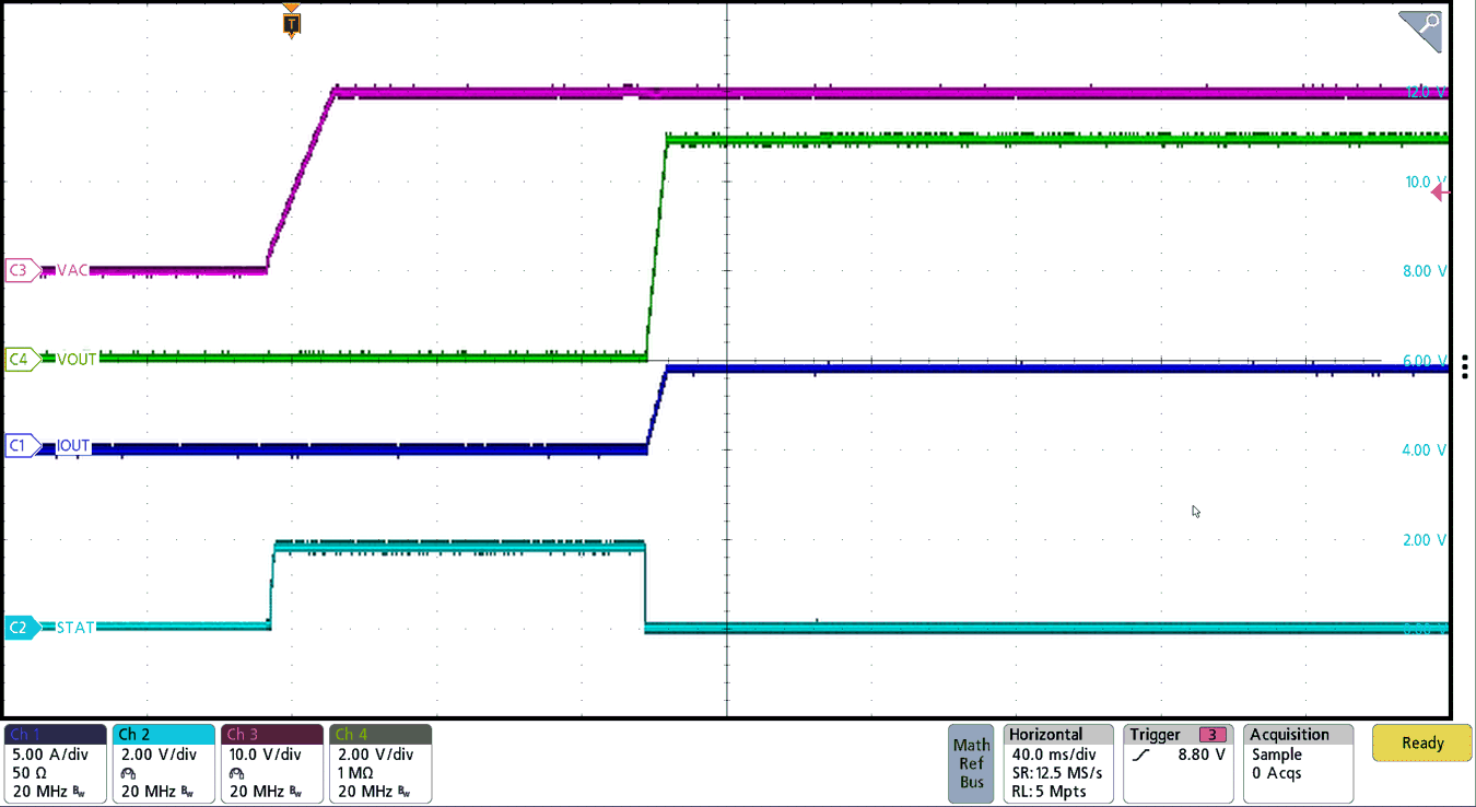
BQ25758A VAC
                        Plug-In Power Up with 5-A Load
VAC = 20 V
Figure 8-3 VAC Plug-In Power Up with 5-A Load
BQ25758A Power
                        Up via I2C with 5-A Load
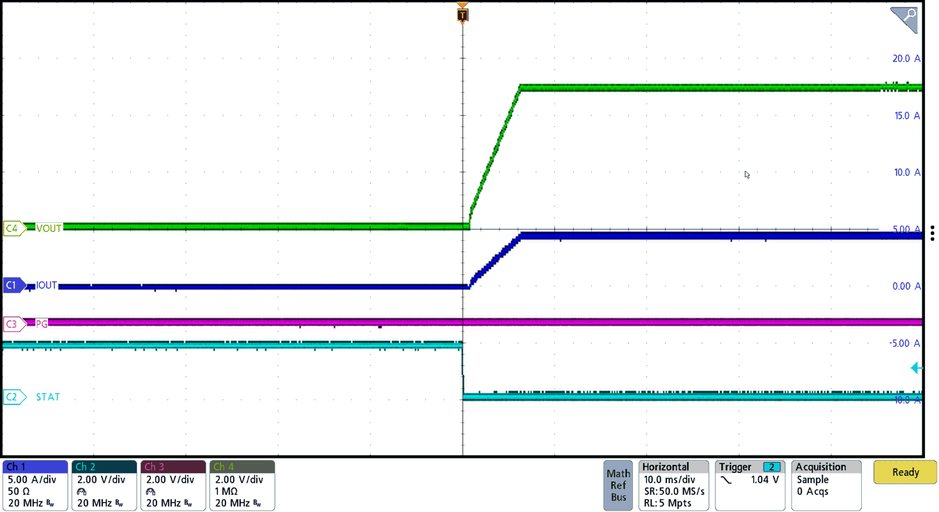
VAC = 20 V
Figure 8-5 Power Up via I2C with 5-A Load
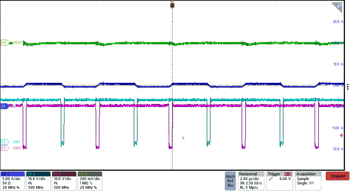
BQ25758A Buck Switching Waveform
VAC = 20 V VOUT = 15 V IOUT = 5 A
Figure 8-7 Buck Switching Waveform
BQ25758A Buck-Boost Switching Waveform
VAC = 20 V VOUT = 20 V IOUT = 5 A
Figure 8-9 Buck-Boost Switching Waveform
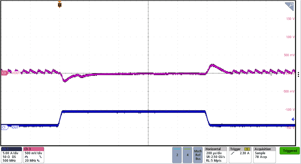
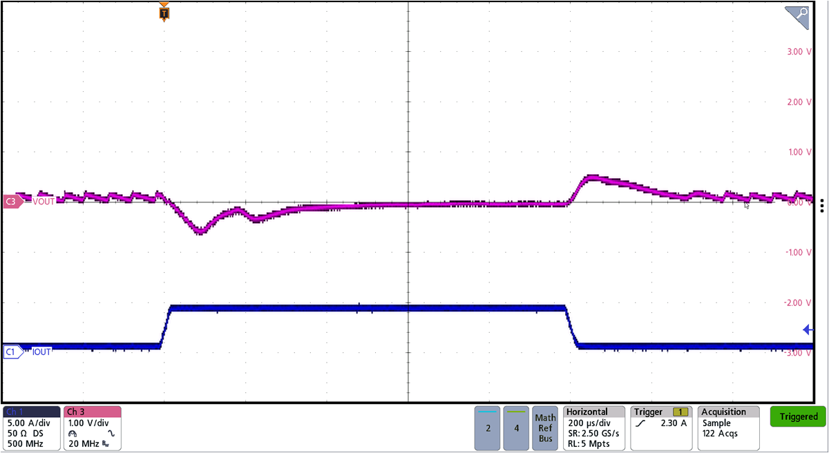
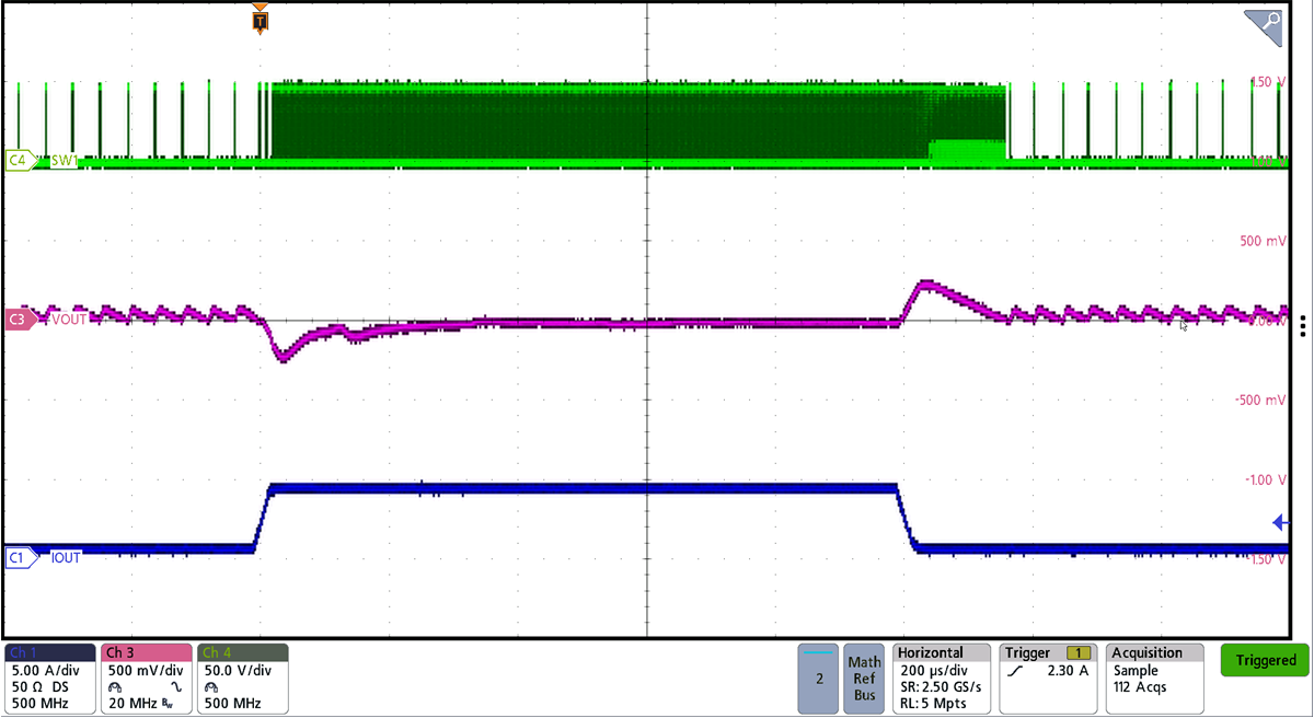
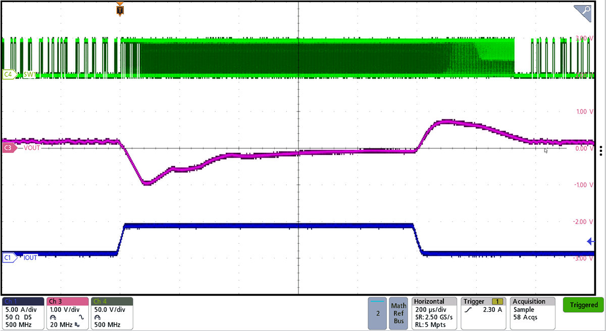
BQ25758A Forward Mode 5-V Transient Reponse with 20 Vin
VAC = 20 V VOUT = 5 V ILOAD = 0.5 A → 4.5 A
Figure 8-11 Forward Mode 5-V Transient Reponse with 20 Vin
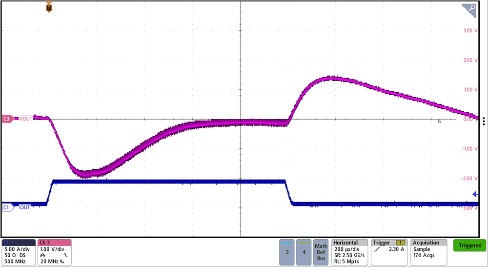
BQ25758A Forward Mode 20-V Transient Reponse with 20 Vin
VAC = 20 V VOUT = 20 V ILOAD = 0.5 A → 4.5 A
Figure 8-13 Forward Mode 20-V Transient Reponse with 20 Vin
BQ25758A Forward Mode 28-V Transient Reponse with 20 Vin
VAC = 20 V VOUT = 28 V ILOAD = 0.5 A → 4.5 A
Figure 8-15 Forward Mode 28-V Transient Reponse with 20 Vin
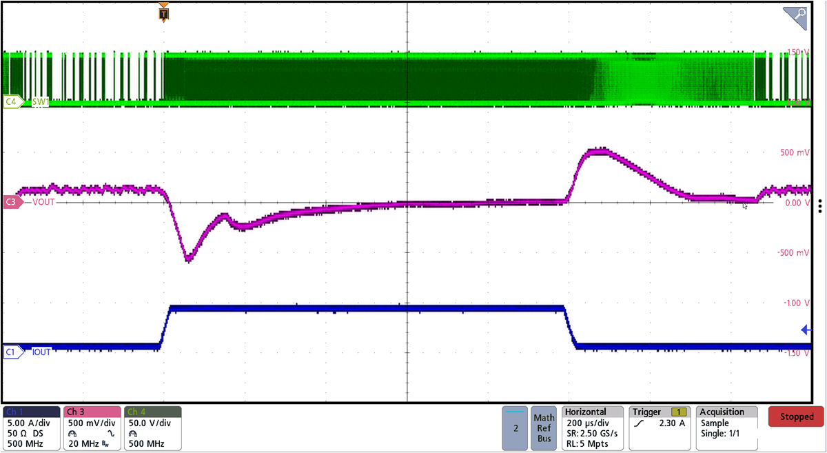
BQ25758A Forward Mode 36-V Transient Reponse with 20 Vin
VAC = 20 V VOUT = 36 V ILOAD = 0.5 A → 4.5 A
Figure 8-17 Forward Mode 36-V Transient Reponse with 20 Vin
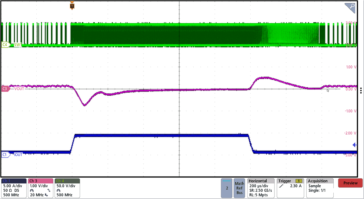
BQ25758A Forward Mode 48-V Transient Reponse with 20 Vin
VAC = 20 V VOUT = 48 V ILOAD = 0.5 A → 4.5 A
Figure 8-19 Forward Mode 48-V Transient Reponse with 20 Vin
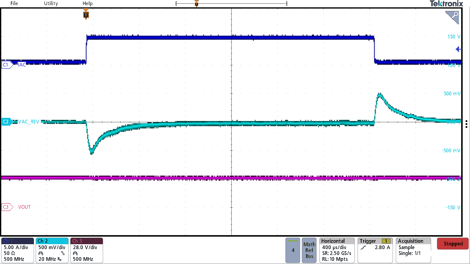
BQ25758A Reverse Mode Power Up with 4-A Load
VOUT = 24 V VAC_REV = 20 V ILOAD = 4 A
Figure 8-21 Reverse Mode Power Up with 4-A Load
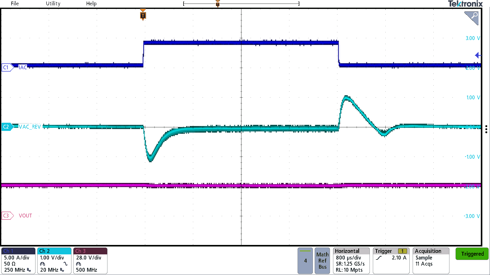
BQ25758A Reverse Mode Buck-Boost Transient Reponse
VOUT = 28 V VAC_REV = 28 V ILOAD = 0.5 A → 4.5 A
Figure 8-23 Reverse Mode Buck-Boost Transient Reponse
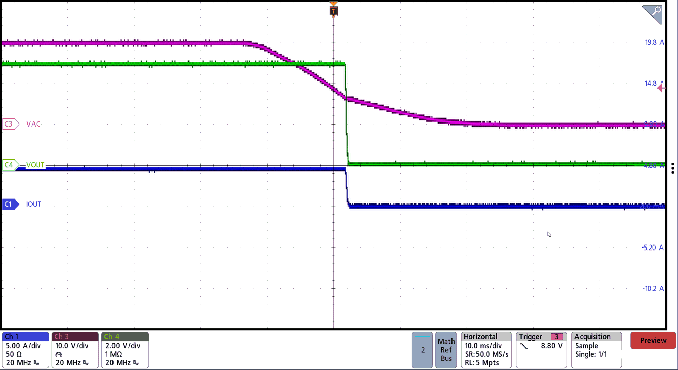
BQ25758A VAC
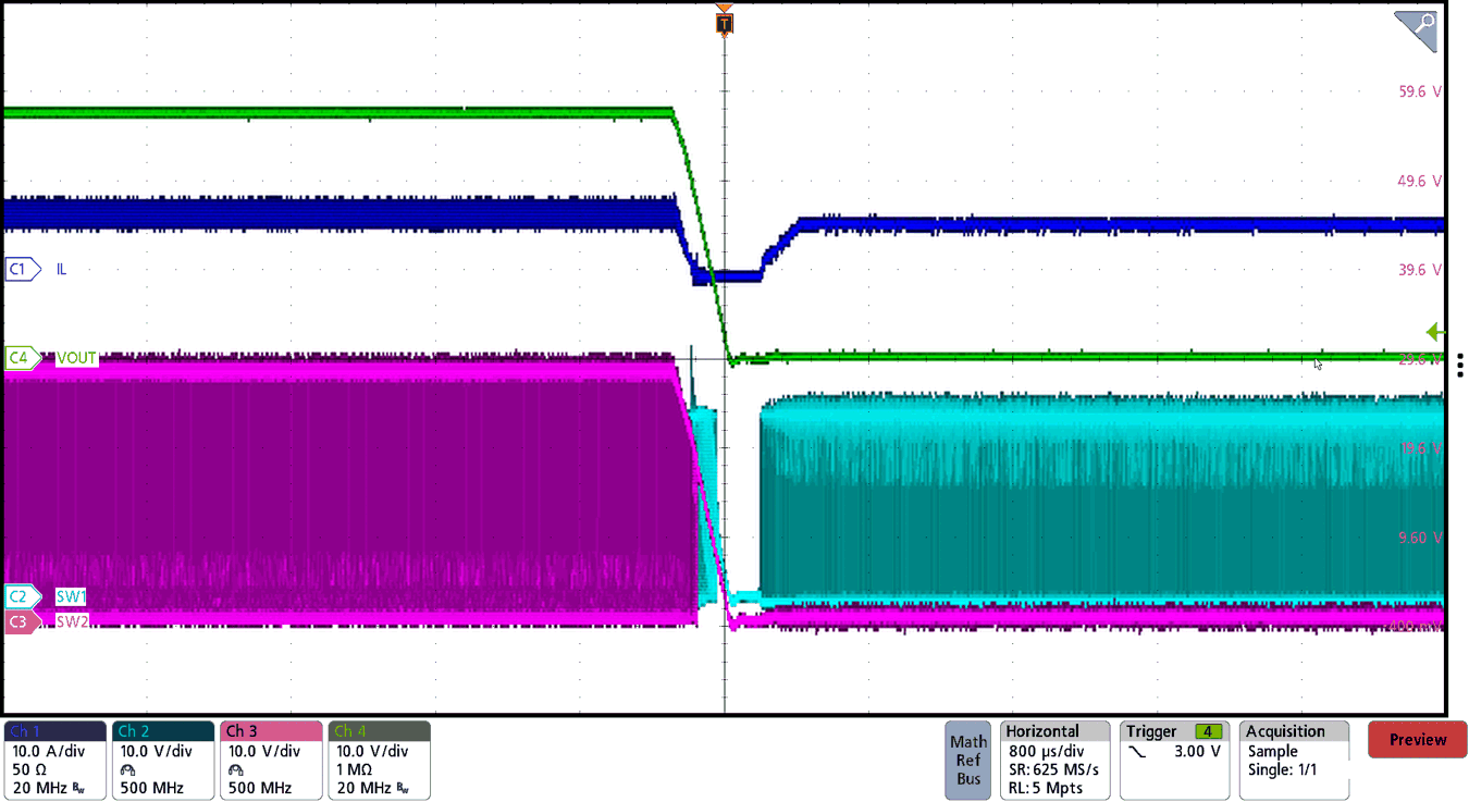
                        Unplug Power Down with 5-A Load
VAC = 20 V → 0 V
Figure 8-4 VAC Unplug Power Down with 5-A Load
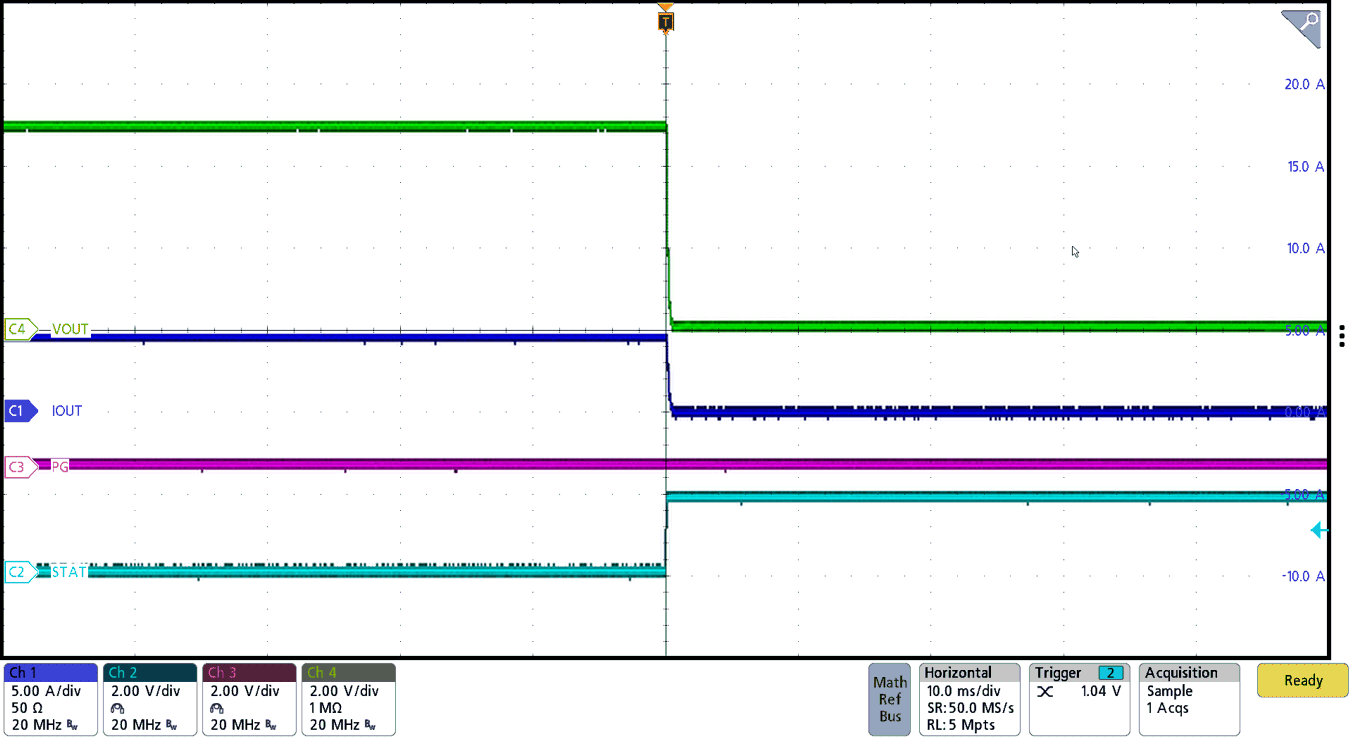
BQ25758A Power
                        Down via I2C with 5-A Load
VAC = 20 V
Figure 8-6 Power Down via I2C with 5-A Load
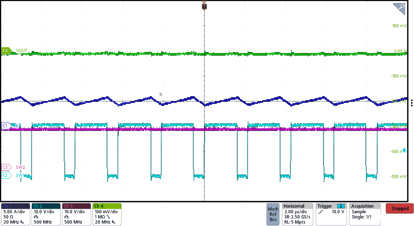
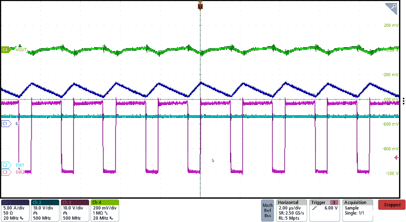
BQ25758A Boost
                        Switching Waveform
VAC = 20 V VOUT = 28 V IOUT = 5 A
Figure 8-8 Boost Switching Waveform
BQ25758A Output Short Circuit Response
VAC = 20 V
Figure 8-10 Output Short Circuit Response
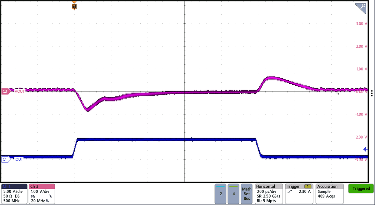
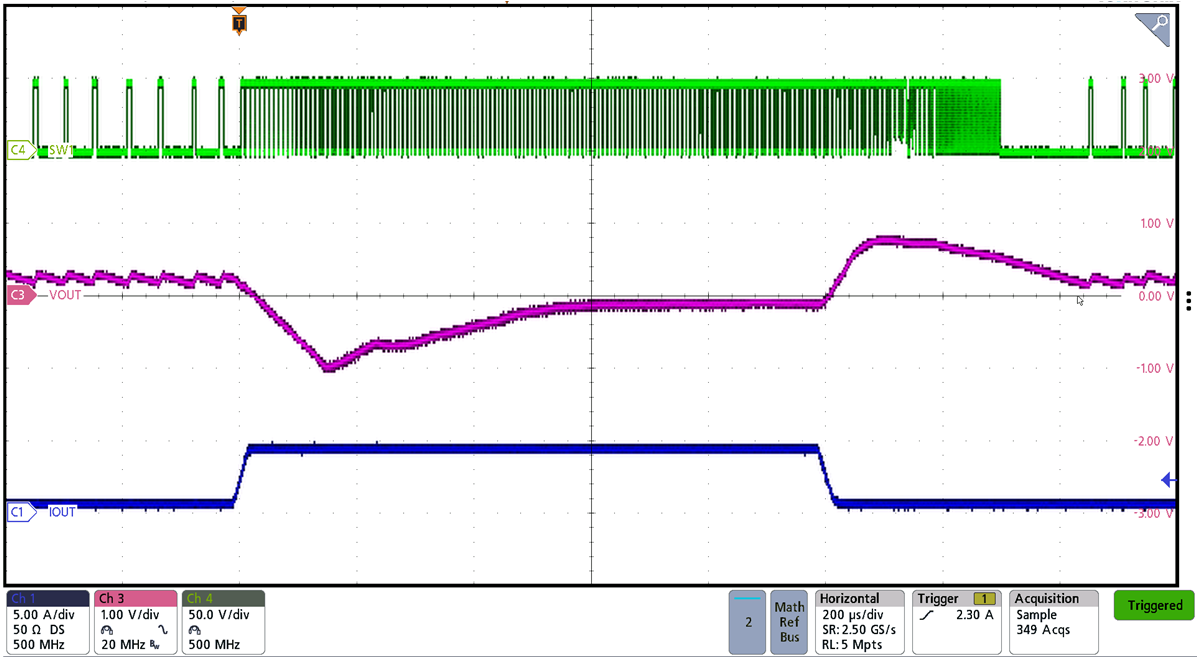
BQ25758A Forward Mode 5-V Transient Reponse with 48 Vin
VAC = 48 V VOUT = 5 V ILOAD = 0.5 A → 4.5 A
Figure 8-12 Forward Mode 5-V Transient Reponse with 48 Vin
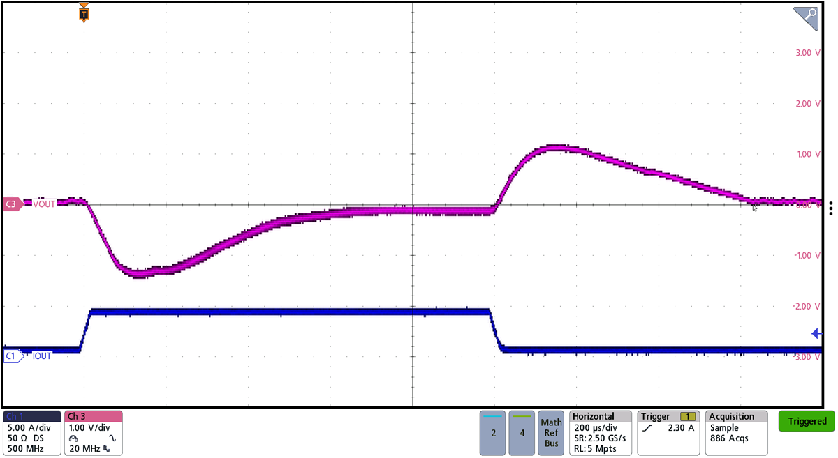
BQ25758A Forward Mode 20-V Transient Reponse with 48 Vin
VAC = 48 V VOUT = 20 V ILOAD = 0.5 A → 4.5 A
Figure 8-14 Forward Mode 20-V Transient Reponse with 48 Vin
BQ25758A Forward Mode 28-V Transient Reponse with 48 Vin
VAC = 48 V VOUT = 28 V ILOAD = 0.5 A → 4.5 A
Figure 8-16 Forward Mode 28-V Transient Reponse with 48 Vin
BQ25758A Forward Mode 36-V Transient Reponse with 48 Vin
VAC = 48 V VOUT = 36 V ILOAD = 0.5 A → 4.5 A
Figure 8-18 Forward Mode 36-V Transient Reponse with 48 Vin
BQ25758A Forward Mode 48-V Transient Reponse with 48 Vin
VAC = 48 V VOUT = 48 V ILOAD = 0.5 A → 4.5 A
Figure 8-20 Forward Mode 48-V Transient Reponse with 48 Vin
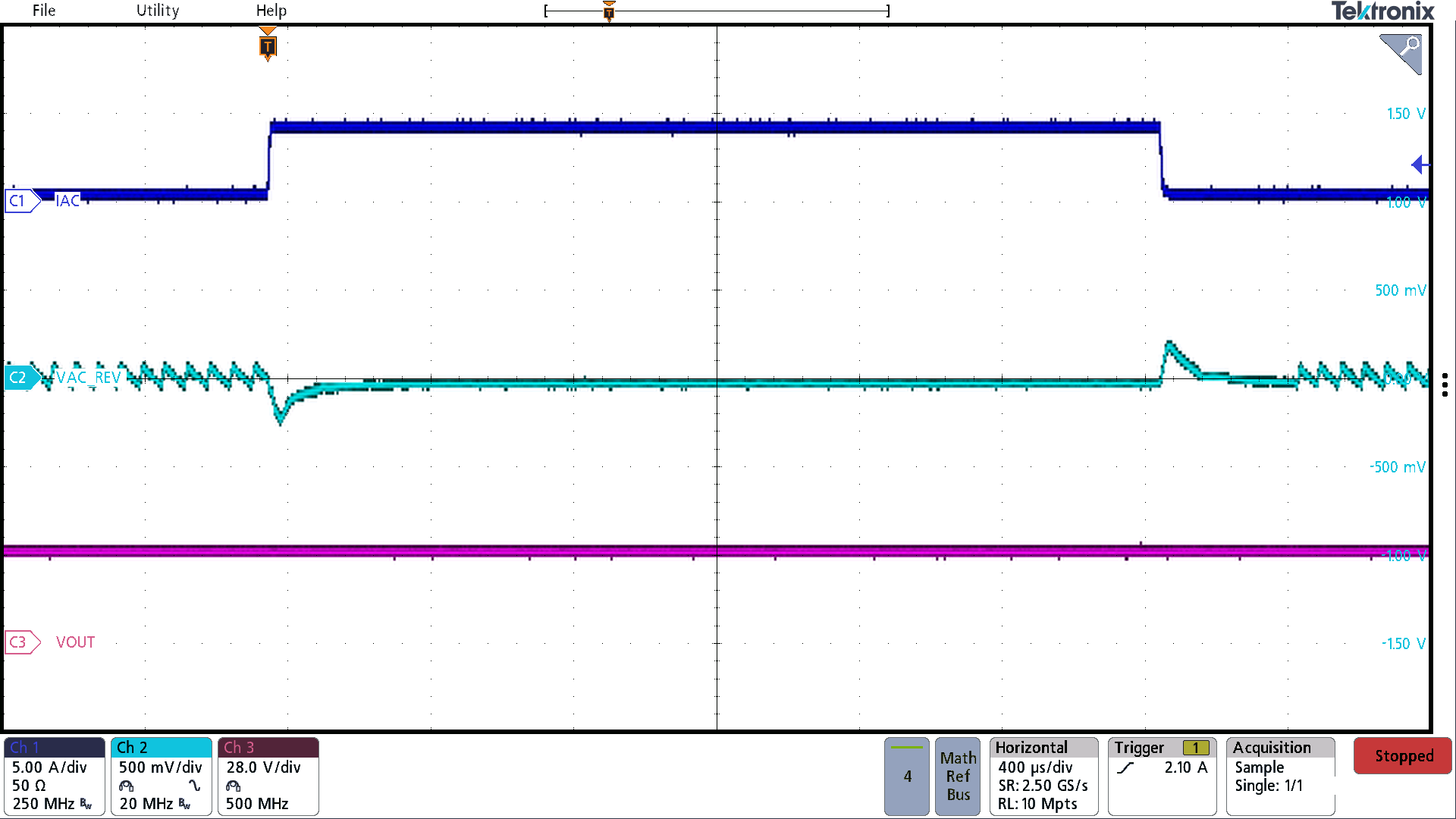
BQ25758A Reverse Mode Buck Transient Reponse
VOUT = 28 V VAC_REV = 5 V ILOAD = 0.5 A → 4.5 A
Figure 8-22 Reverse Mode Buck Transient Reponse
BQ25758A Reverse Mode Boost Transient Reponse
VOUT = 28 V VAC_REV = 48 V ILOAD = 0.5 A → 4.5 A
Figure 8-24 Reverse Mode Boost Transient Reponse