SLUSEK7 September 2024 BQ25773
PRODUCTION DATA
- 1
- 1 Features
- 2 Applications
- 3 Description
- 4 Device Comparison Table
- 5 Pin Configuration and Functions
- 6 Specifications
-
7 Detailed Description
- 7.1 Overview
- 7.2 Functional Block Diagram
- 7.3
Feature Description
- 7.3.1 Power-Up Sequence
- 7.3.2 MODE Pin Detection
- 7.3.3 REGN Regulator (REGN LDO)
- 7.3.4 Independent Comparator Function
- 7.3.5 Battery Charging Management
- 7.3.6 Temperature Regulation (TREG)
- 7.3.7 Vmin Active Protection (VAP) When Battery Only Mode
- 7.3.8 Two Level Battery Discharge Current Limit
- 7.3.9 Fast Role Swap Feature
- 7.3.10 CHRG_OK Indicator
- 7.3.11 Input and Charge Current Sensing
- 7.3.12 Input Current and Voltage Limit Setup
- 7.3.13 Battery Cell Configuration
- 7.3.14 Device HIZ State
- 7.3.15 USB On-The-Go (OTG)
- 7.3.16 Quasi Dual Phase Converter Operation
- 7.3.17 Continuous Conduction Mode (CCM)
- 7.3.18 Pulse Frequency Modulation (PFM)
- 7.3.19 Switching Frequency and Dithering Feature
- 7.3.20 Current and Power Monitor
- 7.3.21 Input Source Dynamic Power Management
- 7.3.22 Integrated 16-Bit ADC for Monitoring
- 7.3.23 Input Current Optimizer (ICO)
- 7.3.24 Two-Level Adapter Current Limit (Peak Power Mode)
- 7.3.25 Processor Hot Indication
- 7.3.26
Device Protection
- 7.3.26.1 Watchdog Timer (WD)
- 7.3.26.2 Input Overvoltage Protection (ACOV)
- 7.3.26.3 Input Overcurrent Protection (ACOC)
- 7.3.26.4 System Overvoltage Protection (SYSOVP)
- 7.3.26.5 Battery Overvoltage Protection (BATOVP)
- 7.3.26.6 Battery Charge Overcurrent Protection (BATCOC)
- 7.3.26.7 Battery Discharge Overcurrent Protection (BATDOC)
- 7.3.26.8 BATFET Charge Current Clamp Protection under LDO Regulation Mode
- 7.3.26.9 Sleep Comparator Protection Between VBUS and ACP_A (SC_VBUSACP)
- 7.3.26.10 High Duty Buck Exit Comparator Protection (HDBCP)
- 7.3.26.11 REGN Power Good Protection (REGN_PG)
- 7.3.26.12 System Under Voltage Lockout (VSYS_UVP) and Hiccup Mode
- 7.3.26.13 OTG Mode Over Voltage Protection (OTG_OVP)
- 7.3.26.14 OTG Mode Under Voltage Protection (OTG_UVP)
- 7.3.26.15 Thermal Shutdown (TSHUT)
- 7.4 Device Functional Modes
- 7.5 Programming
- 7.6 BQ25773 Registers
- 8 Application and Implementation
- 9 Power Supply Recommendations
- 10Layout
- 11Device and Documentation Support
- 12Revision History
- 13Mechanical, Packaging, and Orderable Information
パッケージ・オプション
デバイスごとのパッケージ図は、PDF版データシートをご参照ください。
メカニカル・データ(パッケージ|ピン)
- REE|36
サーマルパッド・メカニカル・データ
発注情報
8.2.2.1 Input Snubber and Filter for Voltage Spike Damping
During adapter hot plug-in, the parasitic inductance and input capacitor from the adapter cable form a second order system. The voltage spike at VBUS pin maybe beyond IC maximum voltage rating and damage IC. The input filter must be carefully designed and tested to prevent over voltage event on VBUS pin.
There are several methods to damp or limit the over voltage spike during adapter hot plug-in. An electrolytic capacitor with high ESR as an input capacitor can damp the over voltage spike well below the IC maximum pin voltage rating. A high current capability TVS Zener diode can also limit the over voltage level to an IC safe level. However these two solutions may not have low cost or small size.
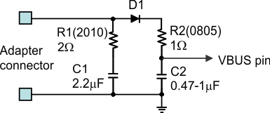
A cost effective and small size solution is shown in Figure 8-2. The R1 and C1 are composed of a damping RC network to damp the hot plug-in oscillation. As a result the over voltage spike is limited to a safe level. D1 is used for reverse voltage protection for VBUS pin. C2 is VBUS pin decoupling capacitor and it should be placed as close as possible to VBUS pin. C2 value should be less than C1 value so R1 can dominate the equivalent ESR value to get enough damping effect. R2 is used to limit inrush current of D1 to prevent D1 getting damage when adapter hot plug-in. R2 and C2 should have 10 µs time constant to limit the dv/dt on VBUS pin to reduce inrush current when adapter hot plug in. R1 has high inrush current. R1 package must be sized enough to handle inrush current power loss according to resistor manufacturer’s data sheet. The filter components' value always need to be verified with real application and minor adjustments may need to fit in the real application circuit.
 Figure 8-2 Input Filter