JAJSGO0C
February 2018 – September 2019
BQ25882
PRODUCTION DATA.
1
特長
2
アプリケーション
3
概要
概略回路図
Device Images
4
改訂履歴
5
Device Comparison Table
6
Pin Configuration and Functions
Pin Functions
7
Specifications
7.1
Absolute Maximum Ratings
7.2
ESD Ratings
7.3
Recommended Operating Conditions
7.4
Thermal Information
7.5
Electrical Characteristics
7.6
Timing Requirements
7.7
Typical Characteristics
8
Detailed Description
8.1
Overview
8.2
Functional Block Diagram
8.3
Feature Description
8.3.1
Device Power-On-Reset
8.3.2
Device Power Up from Battery without Input Source
8.3.3
Device Power Up from Input Source
8.3.3.1
Poor Source Qualification
8.3.3.2
Input Source Type Detection
8.3.3.2.1
D+/D– Detection Sets Input Current Limit
8.3.3.2.2
Force Input Current Limit Detection
8.3.3.3
Power up REGN Regulator (LDO)
8.3.3.4
Converter Power Up
8.3.4
Input Current Optimizer (ICO)
8.3.5
Buck Mode Operation from Battery (OTG)
8.3.6
Power Path Management
8.3.6.1
Narrow VDC Architecture
8.3.6.2
Dynamic Power Management
8.3.6.3
Supplement Mode
8.3.7
Battery Charging Management
8.3.7.1
Autonomous Charging Cycle
8.3.7.2
Battery Charging Profile
8.3.7.3
Charging Termination
8.3.7.4
Thermistor Qualification
8.3.7.4.1
JEITA Guideline Compliance in Charge Mode
8.3.7.4.2
Cold/Hot Temperature Window in OTG Buck Mode
8.3.7.5
Charging Safety Timer
8.3.8
Integrated 16-Bit ADC for Monitoring
8.3.9
Status Outputs (PG, and INT)
8.3.9.1
Power Good Indicator (PG)
8.3.9.2
Interrupt to Host (INT)
8.3.10
Input Current Limit on ILIM Pin
8.3.11
Voltage and Current Monitoring
8.3.11.1
Voltage and Current Monitoring in Boost Mode
8.3.11.1.1
Input Over-voltage Protection
8.3.11.1.2
Input Under-Voltage Protection
8.3.11.1.3
System Over-Voltage Protection
8.3.11.1.4
System Over-Current Protection
8.3.11.2
Voltage and Current Monitoring in OTG Buck Mode
8.3.11.2.1
VBUS Over-Voltage Protection
8.3.11.2.2
VBUS Over-Current Protection
8.3.12
Thermal Regulation and Thermal Shutdown
8.3.12.1
Thermal Protection in Boost Mode
8.3.12.2
Thermal Protection in OTG Buck Mode
8.3.13
Battery Protection
8.3.13.1
Battery Overvoltage Protection (BATOVP)
8.3.13.2
Battery Over-Discharge Protection
8.3.14
Serial Interface
8.3.14.1
Data Validity
8.3.14.2
START and STOP Conditions
8.3.14.3
Byte Format
8.3.14.4
Acknowledge (ACK) and Not Acknowledge (NACK)
8.3.14.5
Slave Address and Data Direction Bit
8.3.14.6
Single Write and Read
8.3.14.7
Multi-Write and Multi-Read
8.4
Device Functional Modes
8.4.1
Host Mode and Default Mode
8.5
Register Maps
8.5.1
Battery Voltage Regulation Limit Register (Address = 00h) [reset = A0h]
Table 9.
REG00 Register Field Descriptions
8.5.2
Charger Current Limit Register (Address = 01h) [reset = 54h]
Table 10.
REG01 Register Field Descriptions
8.5.3
Input Voltage Limit Register (Address = 02h) [reset = 85h]
Table 11.
REG02 Register Field Descriptions
8.5.4
Input Current Limit Register (Address = 03h) [reset = 39h]
Table 12.
REG03 Register Field Descriptions
8.5.5
Precharge and Termination Current Limit Register (Address = 04h) [reset = 22h]
Table 13.
REG04 Register Field Descriptions
8.5.6
Charger Control 1 Register (Address = 05h) [reset = 9Dh]
Table 14.
REG05 Register Field Descriptions
8.5.7
Charger Control 2 Register (Address = 06h) [reset = 7Dh]
Table 15.
REG06 Register Field Descriptions
8.5.8
Charger Control 3 Register (Address = 07h) [reset = 0Ah]
Table 16.
REG07 Register Field Descriptions
8.5.9
Charger Control 4 Register (Address = 08h) [reset = 0Dh]
Table 17.
REG08 Register Field Descriptions
8.5.10
OTG Control Register (Address = 09h) [reset = F6h]
Table 18.
REG09 Register Field Descriptions
8.5.11
ICO Current Limit Register (Address = 0Ah) [reset = XXh]
Table 19.
REG0A Register Field Descriptions
8.5.12
Charger Status 1 Register (Address = 0Bh) [reset = XXh]
Table 20.
REG0B Register Field Descriptions
8.5.13
Charger Status 2 Register (Address = 0Ch) [reset = XXh]
Table 21.
REG0C Register Field Descriptions
8.5.14
NTC Status Register (Address = 0Dh) [reset = 0Xh]
Table 22.
REG0D Register Field Descriptions
8.5.15
FAULT Status Register (Address = 0Eh) [reset = XXh]
Table 23.
REG0E Register Field Descriptions
8.5.16
Charger Flag 1 Register (Address = 0Fh) [reset = 00h]
Table 24.
REG0F Register Field Descriptions
8.5.17
Charger Flag 2 Register (Address = 10h) [reset = 00h]
Table 25.
REG10 Register Field Descriptions
8.5.18
FAULT Flag Register (Address = 11h) [reset = 00h]
Table 26.
REG11 Register Field Descriptions
8.5.19
Charger Mask 1 Register (Address = 12h) [reset = 00h]
Table 27.
REG12 Register Field Descriptions
8.5.20
Charger Mask 2 Register (Address = 13h) [reset = 00h]
Table 28.
REG13 Register Field Descriptions
8.5.21
FAULT Mask Register (Address = 14h) [reset = 00h]
Table 29.
REG14 Register Field Descriptions
8.5.22
ADC Control Register (Address = 15h) [reset = 30h]
Table 30.
REG15 Register Field Descriptions
8.5.23
ADC Function Disable Register (Address = 16h) [reset = 00h]
Table 31.
REG16 Register Field Descriptions
8.5.24
IBUS ADC 1 Register (Address = 17h) [reset = 00h]
Table 32.
REG17 Register Field Descriptions
8.5.25
IBUS ADC 0 Register (Address = 18h) [reset = 00h]
Table 33.
REG18 Register Field Descriptions
8.5.26
ICHG ADC 1 Register (Address = 19h) [reset = 00h]
Table 34.
REG19 Register Field Descriptions
8.5.27
ICHG ADC 0 Register (Address = 1Ah) [reset = 00h]
Table 35.
REG1A Register Field Descriptions
8.5.28
VBUS ADC 1 Register (Address = 1Bh) [reset = 00h]
Table 36.
REG1B Register Field Descriptions
8.5.29
VBUS ADC 0 Register (Address = 1Ch) [reset = 00h]
Table 37.
REG1C Register Field Descriptions
8.5.30
VBAT ADC 1 Register (Address = 1Dh) [reset = 00h]
Table 38.
REG1D Register Field Descriptions
8.5.31
VBAT ADC 0 Register (Address = 1Eh) [reset = 00h]
Table 39.
REG1E Register Field Descriptions
8.5.32
VSYS ADC 1 Register (Address = 1Fh) [reset = 00h]
Table 40.
REG1F Register Field Descriptions
8.5.33
VSYS ADC 0 Register (Address = 20h) [reset = 00h]
Table 41.
REG20 Register Field Descriptions
8.5.34
TS ADC 1 Register (Address = 21h) [reset = 00h]
Table 42.
REG21 Register Field Descriptions
8.5.35
TS ADC 0 Register (Address = 22h) [reset = 00h]
Table 43.
REG22 Register Field Descriptions
8.5.36
TDIE ADC 1 Register (Address = 23h) [reset = 00h]
Table 44.
REG23 Register Field Descriptions
8.5.37
TDIE ADC 0 Register (Address = 24h) [reset = 00h]
Table 45.
REG24 Register Field Descriptions
8.5.38
Part Information Register (Address = 25h) [reset = 11h]
Table 46.
REG25 Register Field Descriptions
9
Application and Implementation
9.1
Application Information
9.2
Typical Application
9.2.1
Design Requirements
9.2.2
Detailed Design Procedure
9.2.2.1
Inductor Selection
9.2.2.2
Input (VBUS / PMID) Capacitor
9.2.2.3
Output (VSYS) Capacitor
9.2.3
Application Curves
10
Power Supply Recommendations
11
Layout
11.1
Layout Guidelines
11.2
Layout Example
12
デバイスおよびドキュメントのサポート
12.1
デバイス・サポート
12.1.1
デベロッパー・ネットワークの製品に関する免責事項
12.1.1.1
デベロッパー・ネットワークの製品に関する免責事項
12.2
ドキュメントのサポート
12.2.1
関連資料
12.3
ドキュメントの更新通知を受け取る方法
12.4
コミュニティ・リソース
12.5
商標
12.6
静電気放電に関する注意事項
12.7
Glossary
13
メカニカル、パッケージ、および注文情報
パッケージ・オプション
メカニカル・データ(パッケージ|ピン)
YFF|25
MXBG083Y
サーマルパッド・メカニカル・データ
発注情報
jajsgo0c_oa
jajsgo0c_pm
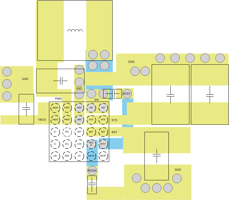
11.2
Layout Example
Figure 92.
PCB Layout Example