JAJSFD7C July   2015  – May 2018

PRODUCTION DATA.  

  1. 特長
  2. アプリケーション
  3. 概要
    1.     概略回路図
  4. 改訂履歴
  5. 概要(続き)
  6. Device Comparison Table
  7. Pin Configuration and Functions
    1.     Pin Functions
  8. Specifications
    1. 8.1 Absolute Maximum Ratings
    2. 8.2 ESD Ratings
    3. 8.3 Recommended Operating Conditions
    4. 8.4 Thermal Information
    5. 8.5 Electrical Characteristics
    6. 8.6 Timing Requirements
    7. 8.7 Typical Characteristics
  9. Detailed Description
    1. 9.1 Functional Block Diagram
    2. 9.2 Feature Description
      1. 9.2.1  Device Power-On-Reset (POR)
      2. 9.2.2  Device Power Up from Battery without Input Source
      3. 9.2.3  Device Power Up from Input Source
        1. 9.2.3.1 Power Up REGN Regulation (LDO)
        2. 9.2.3.2 Poor Source Qualification
        3. 9.2.3.3 Input Source Type Detection
          1. 9.2.3.3.1 PSEL Pins Set Input Current Limit
          2. 9.2.3.3.2 Force Input Current Limit Detection
        4. 9.2.3.4 Input Voltage Limit Threshold Setting (VINDPM Threshold)
        5. 9.2.3.5 Converter Power-Up
      4. 9.2.4  Input Current Optimizer (ICO)
      5. 9.2.5  Boost Mode Operation from Battery
      6. 9.2.6  Power Path Management
        1. 9.2.6.1 Narrow VDC Architecture
        2. 9.2.6.2 Dynamic Power Management
        3. 9.2.6.3 Supplement Mode
      7. 9.2.7  Battery Charging Management
        1. 9.2.7.1 Autonomous Charging Cycle
        2. 9.2.7.2 Battery Charging Profile
        3. 9.2.7.3 Charging Termination
        4. 9.2.7.4 Resistance Compensation (IRCOMP)
        5. 9.2.7.5 Thermistor Qualification
          1. 9.2.7.5.1 JEITA Guideline Compliance in Charge Mode
          2. 9.2.7.5.2 Cold/Hot Temperature Window in Boost Mode
        6. 9.2.7.6 Charging Safety Timer
      8. 9.2.8  Battery Monitor
      9. 9.2.9  Status Outputs (PG, STAT, and INT)
        1. 9.2.9.1 Power Good Indicator (PG)
        2. 9.2.9.2 Charging Status Indicator (STAT)
        3. 9.2.9.3 Interrupt to Host (INT)
      10. 9.2.10 BATET (Q4) Control
        1. 9.2.10.1 BATFET Disable Mode (Shipping Mode)
        2. 9.2.10.2 BATFET Enable (Exit Shipping Mode)
        3. 9.2.10.3 BATFET Full System Reset
      11. 9.2.11 Current Pulse Control Protocol
      12. 9.2.12 Input Current Limit on ILIM
      13. 9.2.13 Thermal Regulation and Thermal Shutdown
        1. 9.2.13.1 Thermal Protection in Buck Mode
        2. 9.2.13.2 Thermal Protection in Boost Mode
      14. 9.2.14 Voltage and Current Monitoring in Buck and Boost Mode
        1. 9.2.14.1 Voltage and Current Monitoring in Buck Mode
          1. 9.2.14.1.1 Input Overvoltage (ACOV)
          2. 9.2.14.1.2 System Overvoltage Protection (SYSOVP)
        2. 9.2.14.2 Current Monitoring in Boost Mode
          1. 9.2.14.2.1 VBUS Overcurrent Protection
          2. 9.2.14.2.2 Boost Mode Overvoltage Protection
      15. 9.2.15 Battery Protection
        1. 9.2.15.1 Battery Overvoltage Protection (BATOVP)
        2. 9.2.15.2 Battery Over-Discharge Protection
        3. 9.2.15.3 System Overcurrent Protection
      16. 9.2.16 Serial Interface
        1. 9.2.16.1 Data Validity
        2. 9.2.16.2 START and STOP Conditions
        3. 9.2.16.3 Byte Format
        4. 9.2.16.4 Acknowledge (ACK) and Not Acknowledge (NACK)
        5. 9.2.16.5 Slave Address and Data Direction Bit
        6. 9.2.16.6 Single Read and Write
        7. 9.2.16.7 Multi-Read and Multi-Write
    3. 9.3 Device Functional Modes
      1. 9.3.1 Host Mode and Default Mode
    4. 9.4 Register Maps
      1. 9.4.1  REG00
        1. Table 6. REG00
      2. 9.4.2  REG01
        1. Table 7. REG01
      3. 9.4.3  REG02
        1. Table 8. REG02
      4. 9.4.4  REG03
        1. Table 9. REG03
      5. 9.4.5  REG04
        1. Table 10. REG04
      6. 9.4.6  REG05
        1. Table 11. REG05
      7. 9.4.7  REG06
        1. Table 12. REG06
      8. 9.4.8  REG07
        1. Table 13. REG07
      9. 9.4.9  REG08
        1. Table 14. REG08
      10. 9.4.10 REG09
        1. Table 15. REG09
      11. 9.4.11 REG0A
        1. Table 16. REG0A
      12. 9.4.12 REG0B
        1. Table 17. REG0B
      13. 9.4.13 REG0C
        1. Table 18. REG0C
      14. 9.4.14 REG0D
        1. Table 19. REG0D
      15. 9.4.15 REG0E
        1. Table 20. REG0E
      16. 9.4.16 REG0F
        1. Table 21. REG0F
      17. 9.4.17 REG10
        1. Table 22. REG10
      18. 9.4.18 REG11
        1. Table 23. REG11
      19. 9.4.19 REG12
        1. Table 24. REG12
      20. 9.4.20 REG13
        1. Table 25. REG13
      21. 9.4.21 REG14
        1. Table 26. REG14
  10. 10Application and Implementation
    1. 10.1 Application Information
    2. 10.2 Typical Application
      1. 10.2.1 Design Requirements
      2. 10.2.2 Detailed Design Procedure
        1. 10.2.2.1 Inductor Selection
        2. 10.2.2.2 Buck Input Capacitor
        3. 10.2.2.3 System Output Capacitor
      3. 10.2.3 Application Curves
    3. 10.3 System Examples
  11. 11Power Supply Recommendations
  12. 12Layout
    1. 12.1 Layout Guidelines
    2. 12.2 Layout Example
  13. 13デバイスおよびドキュメントのサポート
    1. 13.1 ドキュメントのサポート
      1. 13.1.1 関連資料
    2. 13.2 ドキュメントの更新通知を受け取る方法
    3. 13.3 コミュニティ・リソース
    4. 13.4 商標
    5. 13.5 静電気放電に関する注意事項
    6. 13.6 Glossary
  14. 14メカニカル、パッケージ、および注文情報

パッケージ・オプション

メカニカル・データ(パッケージ|ピン)
サーマルパッド・メカニカル・データ
発注情報

Host Mode and Default Mode

The device is a host controlled charger, but it can operate in default mode without host management. In default mode, the device can be used an autonomous charger with no host or while host is in sleep mode. When the charger is in default mode, WATCHDOG_FAULT bit is HIGH. When the charger is in host mode, WATCHDOG_FAULT bit is LOW.

After power-on-reset, the device starts in default mode with watchdog timer expired, or default mode. All the registers are in the default settings.

In default mode, the device keeps charging the battery with 12-hour fast charging safety timer. At the end of the 12-hour, the charging is stopped and the buck converter continues to operate to supply system load. Any write command to device transitions the charger from default mode to host mode. All the device parameters can be programmed by the host. To keep the device in host mode, the host has to reset the watchdog timer by writing 1 to WD_RST bit before the watchdog timer expires (WATCHDOG_FAULT bit is set), or disable watchdog timer by setting WATCHDOG bits=00.

When the watchdog timer (WATCHDOG_FAULT bit = 1) is expired, the device returns to default mode and all registers are reset to default values except IINLIM, VINDPM, VINDPM_OS, BATFET_RST_EN, BATFET_DLY, and BATFET_DIS bits.
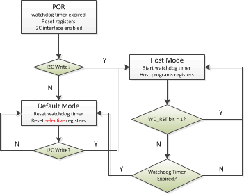
bq25896 Wathdog_timer_flowchart_slusbu7.gifFigure 24. Watchdog Timer Flow Chart