JAJSSA6 December   2023 BQ25960H

PRODUCTION DATA  

  1.   1
  2. 特長
  3. アプリケーション
  4. 概要
  5. 概要 (続き)
  6. Device Comparison Table
  7. Pin Configuration and Functions
  8. Specifications
    1. 7.1 Absolute Maximum Ratings
    2. 7.2 ESD Ratings
    3. 7.3 Recommended Operating Conditions
    4. 7.4 Thermal Information
    5. 7.5 Electrical Characteristics
    6. 7.6 Timing Requirements
    7. 7.7 Typical Characteristics
  9. Detailed Description
    1. 8.1 Overview
    2. 8.2 Functional Block Diagram
    3. 8.3 Feature Description
      1. 8.3.1  Charging System
      2. 8.3.2  Battery Charging Profile
      3. 8.3.3  Device Power Up
      4. 8.3.4  Device HIZ State
      5. 8.3.5  Dual Input Bi-Directional Power Path Management
        1. 8.3.5.1 ACDRV Turn-On Condition
        2. 8.3.5.2 Single Input from VAC to VBUS without ACFET-RBFET
        3. 8.3.5.3 Single Input with ACFET1
        4. 8.3.5.4 Dual Input with ACFET1-RBFET1
        5. 8.3.5.5 Dual Input with ACFET1-RBFET1 and ACFET2-RBFET2
        6. 8.3.5.6 OTG and Reverse TX Mode Operation
      6. 8.3.6  Bypass Mode Operation
      7. 8.3.7  Charging Start-Up
      8. 8.3.8  Adapter Removal
      9. 8.3.9  Integrated 16-Bit ADC for Monitoring and Smart Adapter Feedback
      10. 8.3.10 Device Modes and Protection Status
        1. 8.3.10.1 Input Overvoltage, Overcurrent, Undercurrent, Reverse-Current and Short-Circuit Protection
        2. 8.3.10.2 Battery Overvoltage and Overcurrent Protection
        3. 8.3.10.3 IC Internal Thermal Shutdown, TSBUS, and TSBAT Temperature Monitoring
      11. 8.3.11 INT Pin, STAT, FLAG, and MASK Registers
      12. 8.3.12 Dual Charger Operation Using Primary and Secondary Modes
      13. 8.3.13 CDRVH and CDRVL_ADDRMS Functions
    4. 8.4 Programming
      1. 8.4.1 F/S Mode Protocol
    5. 8.5 Register Maps
      1. 8.5.1 I2C Registers
  10. Application and Implementation
    1. 9.1 Application Information
    2. 9.2 Typical Application
      1. 9.2.1 Standalone Application Information (for use with main charger)
        1. 9.2.1.1 Design Requirements
        2. 9.2.1.2 Detailed Design Procedure
        3. 9.2.1.3 Application Curves
  11. 10Power Supply Recommendations
  12. 11Layout
    1. 11.1 Layout Guidelines
    2. 11.2 Layout Example
  13. 12Device and Documentation Support
    1. 12.1 Device Support
      1. 12.1.1 サード・パーティ製品に関する免責事項
    2. 12.2 Documentation Support
      1. 12.2.1 Related Documentation
    3. 12.3 ドキュメントの更新通知を受け取る方法
    4. 12.4 サポート・リソース
    5. 12.5 Trademarks
    6. 12.6 静電気放電に関する注意事項
    7. 12.7 用語集
  14. 13Revision History
  15. 14Mechanical, Packaging, and Orderable Information
    1. 14.1 Package Option Addendum
    2. 14.2 Tape and Reel Information

パッケージ・オプション

メカニカル・データ(パッケージ|ピン)
サーマルパッド・メカニカル・データ
発注情報

Charging System

BQ25960H is a single-cell high efficiency switched cap charger, used in parallel with a switching mode charger. A host must set up the protections and alarms on BQ25960H prior to enabling the BQ25960H. The host must monitor the alarms generated by BQ25960H and communicate with the smart adapter to control the current delivered to the charger.
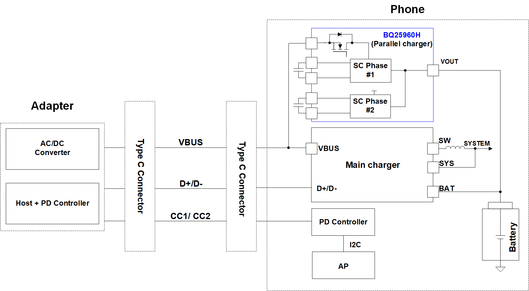
GUID-20231122-SS0I-PFKW-MWCR-WXCCJR4PVVJR-low.gif Figure 8-1 BQ25960H System Diagram