SLUS696C June   2006  – February 2019

PRODUCTION DATA.  

  1. Features
  2. Applications
  3. Description
    1.     Device Images
      1.      Simplified Schematic
  4. Revision History
  5. Pin Configuration and Functions
    1.     Pin Functions
  6. Specifications
    1. 6.1 Absolute Maximum Ratings
    2. 6.2 ESD Ratings
    3. 6.3 Recommended Operating Conditions
    4. 6.4 Thermal Information
    5. 6.5 Electrical Characteristics
    6. 6.6 Standard Serial Communication (SDQ) Timing
    7. 6.7 OTP Programming Specifications
    8. 6.8 Typical Characteristics
  7. Detailed Description
    1. 7.1 Overview
    2. 7.2 Functional Block Diagram
    3. 7.3 Feature Description
      1. 7.3.1 Non-Volatile Memory
      2. 7.3.2 Authentication
      3. 7.3.3 Communication and Power
    4. 7.4 Device Functional Modes
      1. 7.4.1 Profile Command
      2. 7.4.2 Sleep Mode Description
    5. 7.5 Programming
      1. 7.5.1 Communicating with the bq26100 Device
      2. 7.5.2 Memory Descriptions
        1. 7.5.2.1 Non-Volatile OTP Memory
          1. 7.5.2.1.1 General Use – Memory Function Commands 0xF0 (Read) and 0x0F (Write)
          2. 7.5.2.1.2 General Use — Memory Function Commands 0xFA (Read) and 0xAF (Write)
          3. 7.5.2.1.3 Status – Memory Function Commands 0xAA (Read) and 0x55 (Write)
            1. 7.5.2.1.3.1 PAGE LOCK (offset = D431h) [reset = 0h]
              1. Table 5. PAGE LOCK Field Descriptions
        2. 7.5.2.2 Non-Volatile EEPROM Memory
          1. 7.5.2.2.1 General Use – Memory Function Commands 0xE0 (Read) and 0x0E (Write)
      3. 7.5.3 SHA-1 Description
      4. 7.5.4 Key Programming Description
    6. 7.6 Register Maps
      1. 7.6.1 Volatile Register Memory
        1. 7.6.1.1 Message and Digest Registers – Memory Function Command 0xDD (Read) and 0x22 (Write)
        2. 7.6.1.2 Control and Version Registers – Memory Function Command 0x88 (Read) and 0x77 (Write)
          1. 7.6.1.2.1 CTRL Register (address = 0001h) [reset = 1h]
            1. Table 9. Control Register Field Descriptions
  8. Application and Implementation
    1. 8.1 Application Information
    2. 8.2 Typical Application
      1. 8.2.1 Design Requirements
      2. 8.2.2 Detailed Design Procedure
  9. Power Supply Recommendations
  10. 10Layout
    1. 10.1 Layout Guidelines
    2. 10.2 Layout Example
  11. 11Device and Documentation Support
    1. 11.1 Receiving Notification of Documentation Updates
    2. 11.2 Community Resources
    3. 11.3 Trademarks
    4. 11.4 Electrostatic Discharge Caution
    5. 11.5 Glossary
  12. 12Mechanical, Packaging, and Orderable Information

パッケージ・オプション

メカニカル・データ(パッケージ|ピン)
サーマルパッド・メカニカル・データ
発注情報

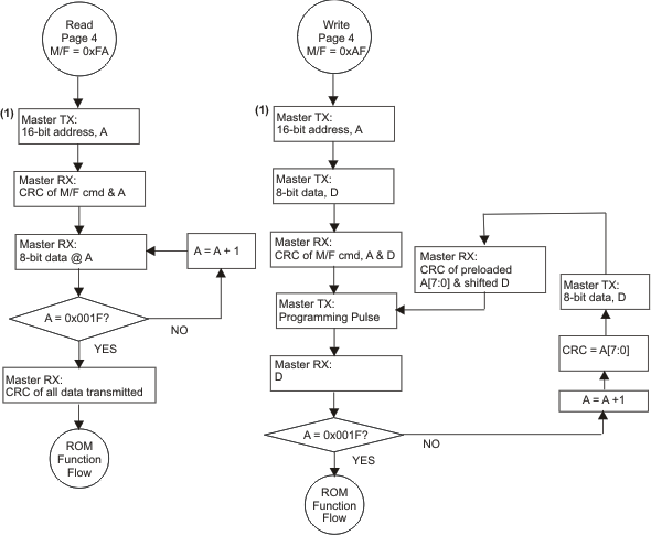
General Use — Memory Function Commands 0xFA (Read) and 0xAF (Write)

The general use space is erased to read 0x00. Data written to the general space is ORed with data already present at the address to be written. A bit can only be flipped from 0 to 1.

Table 3. General Memory Space Addressing

ADDRESSES FUNCTION
0x001F – 0x0000 Page 4 – 32 bytes general use
bq26100 otp_w_r_lus696.gif
16-Bit address is sent with lower 8-bit address followed by higher 8-bit address with least significant bit first.
Figure 13. General Memory OTP Write/Read Flows