SLUS696C
June 2006 – February 2019
PRODUCTION DATA.
1
Features
2
Applications
3
Description
Device Images
Simplified Schematic
4
Revision History
5
Pin Configuration and Functions
Pin Functions
6
Specifications
6.1
Absolute Maximum Ratings
6.2
ESD Ratings
6.3
Recommended Operating Conditions
6.4
Thermal Information
6.5
Electrical Characteristics
6.6
Standard Serial Communication (SDQ) Timing
6.7
OTP Programming Specifications
6.8
Typical Characteristics
7
Detailed Description
7.1
Overview
7.2
Functional Block Diagram
7.3
Feature Description
7.3.1
Non-Volatile Memory
7.3.2
Authentication
7.3.3
Communication and Power
7.4
Device Functional Modes
7.4.1
Profile Command
7.4.2
Sleep Mode Description
7.5
Programming
7.5.1
Communicating with the bq26100 Device
7.5.2
Memory Descriptions
7.5.2.1
Non-Volatile OTP Memory
7.5.2.1.1
General Use – Memory Function Commands 0xF0 (Read) and 0x0F (Write)
7.5.2.1.2
General Use — Memory Function Commands 0xFA (Read) and 0xAF (Write)
7.5.2.1.3
Status – Memory Function Commands 0xAA (Read) and 0x55 (Write)
7.5.2.1.3.1
PAGE LOCK (offset = D431h) [reset = 0h]
Table 5.
PAGE LOCK Field Descriptions
7.5.2.2
Non-Volatile EEPROM Memory
7.5.2.2.1
General Use – Memory Function Commands 0xE0 (Read) and 0x0E (Write)
7.5.3
SHA-1 Description
7.5.4
Key Programming Description
7.6
Register Maps
7.6.1
Volatile Register Memory
7.6.1.1
Message and Digest Registers – Memory Function Command 0xDD (Read) and 0x22 (Write)
7.6.1.2
Control and Version Registers – Memory Function Command 0x88 (Read) and 0x77 (Write)
7.6.1.2.1
CTRL Register (address = 0001h) [reset = 1h]
Table 9.
Control Register Field Descriptions
8
Application and Implementation
8.1
Application Information
8.2
Typical Application
8.2.1
Design Requirements
8.2.2
Detailed Design Procedure
9
Power Supply Recommendations
10
Layout
10.1
Layout Guidelines
10.2
Layout Example
11
Device and Documentation Support
11.1
Receiving Notification of Documentation Updates
11.2
Community Resources
11.3
Trademarks
11.4
Electrostatic Discharge Caution
11.5
Glossary
12
Mechanical, Packaging, and Orderable Information
パッケージ・オプション
メカニカル・データ(パッケージ|ピン)
DRP|6
MPDS168D
サーマルパッド・メカニカル・データ
発注情報
slus696c_oa
6.8
Typical Characteristics
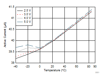
Figure 2.
Active Current Across SDQ Voltage and Temperature (Not Authenticating)
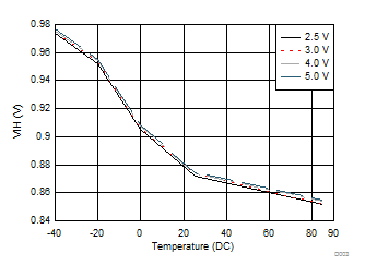
Figure 4.
VIH Across SDQ Voltage and Temperature
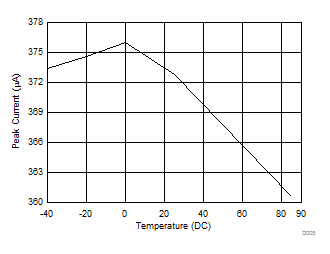
Figure 6.
Peak Current Across Temperature (While Authenticating)
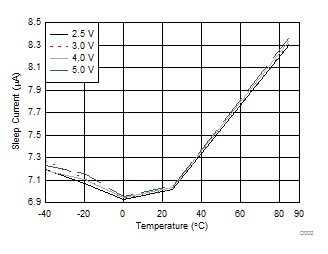
Figure 3.
Sleep Current Across SDQ Voltage and Temperature
Figure 5.
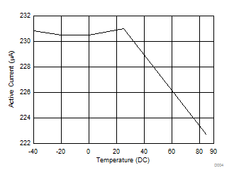
Active Current Across Temperature (While Authenticating)