SLUSB23B October 2012 – June 2015
PRODUCTION DATA.
- 1 Features
- 2 Applications
- 3 Description
- 4 Revision History
- 5 Device Comparison Table
- 6 Pin Configuration and Functions
-
7 Specifications
- 7.1 Absolute Maximum Ratings
- 7.2 ESD Ratings
- 7.3 Recommended Operating Conditions
- 7.4 Thermal Information
- 7.5 Electrical Characteristics: Power-On Reset
- 7.6 2.5-V LDO Regulator
- 7.7 Integrating ADC (Coulomb Counter) Characteristics
- 7.8 Integrated Sense Resistor Characteristics
- 7.9 ADC (Temperature and Cell Measurement) Characteristics
- 7.10 EEPROM Memory Characteristics
- 7.11 Timing Requirements: I2C-Compatible Interface Communication
- 7.12 Typical Characteristics
-
8 Detailed Description
- 8.1 Overview
- 8.2 Functional Block Diagram
- 8.3 Feature Description
- 8.4 Device Functional Modes
- 8.5
Programming
- 8.5.1
Standard Data Commands
- 8.5.1.1
Control(): 0x00 and 0x01
- 8.5.1.1.1 CONTROL_STATUS: 0x0000
- 8.5.1.1.2 DEVICE_TYPE: 0x0001
- 8.5.1.1.3 FW_VERSION: 0x0002
- 8.5.1.1.4 PREV_MACWRITE: 0x0007
- 8.5.1.1.5 CHEM_ID: 0x0008
- 8.5.1.1.6 BAT_INSERT: 0X000C
- 8.5.1.1.7 BAT_REMOVE: 0X000D
- 8.5.1.1.8 SET_HIBERNATE: 0x0011
- 8.5.1.1.9 CLEAR_HIBERNATE: 0x0012
- 8.5.1.1.10 SET_CFGUPDATE: 0x0013
- 8.5.1.1.11 SEALED: 0x0020
- 8.5.1.1.12 RESET: 0x0041
- 8.5.1.1.13 SOFT_RESET: 0x0042
- 8.5.1.2 Temperature( ): 0x02 and 0x03
- 8.5.1.3 Voltage( ): 0x04 and 0x05
- 8.5.1.4 Flags( ): 0x06 and 0x07
- 8.5.1.5 NominalAvailableCapacity( ): 0x08 and 0x09
- 8.5.1.6 FullAvailableCapacity( ): 0x0A and 0x0B
- 8.5.1.7 RemainingCapacity( ): 0x0C and 0x0D
- 8.5.1.8 FullChargeCapacity( ): 0x0E and 0x0F
- 8.5.1.9 AverageCurrent( ): 0x10 and 0x11
- 8.5.1.10 AveragePower( ): 0x18 and 0x19
- 8.5.1.11 StateOfCharge( ): 0x1C and 0x1D
- 8.5.1.12 IntTemperature( ): 0x1E and 0x1F
- 8.5.1.13 StateOfHealth( ): 0x20 and 0x21
- 8.5.1.14 OperationConfiguration( ): 0x3A and 0x3B
- 8.5.1.15 DesignCapacity( ): 0x3C and 0x3D
- 8.5.1.16 DebugX( ):
- 8.5.1.1
Control(): 0x00 and 0x01
- 8.5.2 Extended Data Commands
- 8.5.3 Block Data Interface
- 8.5.4 Access Modes
- 8.5.5 Data Block Summary
- 8.5.6 Detecting Charge Termination
- 8.5.7 Communications
- 8.5.1
Standard Data Commands
- 8.6 Register Maps
- 9 Application and Implementation
- 10Power Supply Recommendations
- 11Layout
- 12Device and Documentation Support
- 13Mechanical, Packaging, and Orderable Information
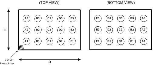
6 Pin Configuration and Functions
YZP Package
15-Pin DSBGA

Pin Functions
| PIN | I/O(1) | DESCRIPTION | |
|---|---|---|---|
| NAME | NO. | ||
| BAT | E2 | I | Cell-voltage measurement input. ADC input. Recommend 4.8 V maximum for conversion accuracy. |
| BIN | C3 | I | Battery-insertion detection input. A logic high-to-low transition is detected as a battery insertion event. Recommend using a pullup resistor >1 MΩ (1.8 MΩ, typical) to VCC for reduced power consumption. An internal pullup resistor option is also available using the Operation Configuration [BI_PU_EN] register bit. |
| CE | D2 | I | Chip Enable. Internal LDO is disconnected from REGIN when driven low. |
| GPOUT | A2 | O | General Purpose open-drain output. May be configured as a Battery Low indicator or perform SOC interrupt (SOC_INT) function. |
| NC | A1, B2 | NA | No internal connection. May be left floating. |
| C2, D3, E3 | IO | Reserved for factory use. Must be left floating for proper operation. | |
| REGIN | E1 | P | Regulator input. Decouple with 0.1-μF ceramic capacitor to VSS. |
| SCL | A3 | I | Slave I2C serial communications clock input line for communication with system (Master). Use with 10-kΩ pullup resistor (typical). |
| SDA | B3 | I/O | Slave I2C serial communications data line for communication with system (Master). Open-drain IO. Use with 10-kΩ pullup resistor (typical). |
| SRX | B1 | IA | Integrated Sense Resistor and Coulomb Counter input typically connected to battery PACK– terminal. For best performance decouple with 0.1-μF ceramic capacitor to VSS. |
| VCC | D1 | P | Regulator output and bq27425 processor power. Decouple with 1-μF ceramic capacitor to VSS. |
| VSS | C1 | P, IA | Device ground and Integrated Sense Resistor termination. |
(1) IO = Digital input/output, IA = Analog input, P = Power connection