JAJSNS5 December 2022 BQ28Z620
PRODUCTION DATA
- 1 特長
- 2 アプリケーション
- 3 概要
- 4 Revision History
- 5 概要 (続き)
- 6 BQ28Z620 Changes from BQ28Z610-R1
- 7 Pin Configuration and Functions
-
8 Specifications
- 8.1 Absolute Maximum Ratings
- 8.2 ESD Ratings
- 8.3 Recommended Operating Conditions
- 8.4 Thermal Information
- 8.5 Supply Current
- 8.6 Power Supply Control
- 8.7 Power-On Reset (POR)
- 8.8 Internal 1.8-V LDO
- 8.9 Current Wake Comparator
- 8.10 Coulomb Counter
- 8.11 ADC Digital Filter
- 8.12 ADC Multiplexer
- 8.13 Cell Balancing Support
- 8.14 Internal Temperature Sensor
- 8.15 NTC Thermistor Measurement Support
- 8.16 High-Frequency Oscillator
- 8.17 Low-Frequency Oscillator
- 8.18 Voltage Reference 1
- 8.19 Voltage Reference 2
- 8.20 Instruction Flash
- 8.21 Data Flash
- 8.22 Current Protection Thresholds
- 8.23 Current Protection Timing
- 8.24 N-CH FET Drive (CHG, DSG)
- 8.25 I2C Interface I/O
- 8.26 I2C Interface Timing
- 8.27 Typical Characteristics
-
9 Detailed Description
- 9.1 Overview
- 9.2 Functional Block Diagram
- 9.3
Feature Description
- 9.3.1 Battery Parameter Measurements
- 9.3.2 Coulomb Counter (CC)
- 9.3.3 CC Digital Filter
- 9.3.4 ADC Multiplexer
- 9.3.5 Analog-to-Digital Converter (ADC)
- 9.3.6 ADC Digital Filter
- 9.3.7 Internal Temperature Sensor
- 9.3.8 External Temperature Sensor Support
- 9.3.9 Power Supply Control
- 9.3.10 Power-On Reset
- 9.3.11 Bus Communication Interface
- 9.3.12 I2C Timeout
- 9.3.13 Cell Balancing Support
- 9.3.14 N-Channel Protection FET Drive
- 9.3.15 Low Frequency Oscillator
- 9.3.16 High Frequency Oscillator
- 9.3.17 1.8-V Low Dropout Regulator
- 9.3.18 Internal Voltage References
- 9.3.19 Overcurrent in Discharge Protection
- 9.3.20 Short-Circuit Current in Charge Protection
- 9.3.21 Short-Circuit Current in Discharge 1 and 2 Protection
- 9.3.22 Primary Protection Features
- 9.3.23 Gas Gauging
- 9.3.24 Charge Control Features
- 9.3.25 Authentication
- 9.4 Device Functional Modes
- 10Applications and Implementation
- 11Power Supply Recommendations
- 12Layout
- 13Device and Documentation Support
- 14Mechanical, Packaging, and Orderable Information
12.1 Layout Guidelines
- The layout for the high-current path begins at the PACK+ pin of the battery pack. As charge current travels through the pack, it finds its way through protection FETs, a chemical fuse, the Li-ion cells and cell connections, and the sense resistor, and then returns to the PACK– pin. In addition, some components are placed across the PACK+ and PACK– pins to reduce effects from electrostatic discharge.
- The N-channel charge and discharge FETs must be selected for a given application. Most portable battery applications are a good option for the CSD16412Q5A. These FETs are rated at 14-A, 25-V device with Rds(on) of 11 mΩ when the gate drive voltage is 10 V. The gates of all protection FETs are pulled to the source with a high-value resistor between the gate and source to ensure they are turned off if the gate drive is open. The capacitors (both 0.1-µF values) placed across the FETs are to help protect the FETs during an ESD event. The use of two devices ensures normal operation if one of them becomes shorted. For effective ESD protection, the copper trace inductance of the capacitor leads must be designed to be as short and wide as possible. Ensure that the voltage rating of both these capacitors is adequate to hold off the applied voltage if one of the capacitors becomes shorted.
- The quality of the Kelvin connections at the sense resistor is critical. The sense resistor must have a temperature coefficient no greater than 50 ppm in order to minimize current measurement drift with temperature. Choose the value of the sense resistor to correspond to the available overcurrent and short-circuit ranges of the BQ28Z620. Select the smallest value possible in order to minimize the negative voltage generated on the BQ28Z620 VSS node(s) during a short circuit. This pin has an absolute minimum of –0.3 V. Parallel resistors can be used as long as good Kelvin sensing is ensured. The device is designed to support a 1-mΩ to 3-mΩ sense resistor.
- A pair of series 0.1-μF ceramic capacitors is placed across the PACK+ and PACK– pins to help in the mitigation of external electrostatic discharges. The two devices in series ensure continued operation of the pack if one of the capacitors becomes shorted. Optionally, a transorb such as the SMBJ2A can be placed across the pins to further improve ESD immunity.
- In reference to the gas gauge circuit the following features require attention for component placement and layout: Differential Low-Pass Filter, I2C communication, and PBI (Power Backup Input).
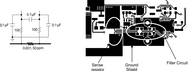
- The BQ28Z620 uses an integrating delta-sigma ADC for current measurements. Add a 100-Ω resistor from the sense resistor to the SRP and SRN inputs of the device. Place a 0.1-μF filter capacitor across the SRP and SRN inputs. Optional 0.1-μF filter capacitors can be added for additional noise filtering for each sense input pin to ground, if required for your circuit. Place all filter components as close as possible to the device. Route the traces from the sense resistor in parallel to the filter circuit. Adding a ground plane around the filter network can add additional noise immunity.
 Figure 12-1 BQ28Z620 Differential Filter
- The BQ28Z620 has an internal LDO that is internally compensated and does not require an external decoupling capacitor. The PBI pin is used as a power supply backup input pin, providing power during brief transient power outages. A standard 2.2-μF ceramic capacitor is connected from the PBI pin to ground, as shown in application example.
- The I2C clock and data pins have integrated high-voltage ESD protection circuits; however, adding a Zener diode and series resistor provides more robust ESD performance. The I2C clock and data lines have an internal pull-down. When the gas gauge senses that both lines are low (such as during removal of the pack), the device performs auto-offset calibration and then goes into SLEEP mode to conserve power.