JAJSNS5 December 2022 BQ28Z620
PRODUCTION DATA
- 1 特長
- 2 アプリケーション
- 3 概要
- 4 Revision History
- 5 概要 (続き)
- 6 BQ28Z620 Changes from BQ28Z610-R1
- 7 Pin Configuration and Functions
-
8 Specifications
- 8.1 Absolute Maximum Ratings
- 8.2 ESD Ratings
- 8.3 Recommended Operating Conditions
- 8.4 Thermal Information
- 8.5 Supply Current
- 8.6 Power Supply Control
- 8.7 Power-On Reset (POR)
- 8.8 Internal 1.8-V LDO
- 8.9 Current Wake Comparator
- 8.10 Coulomb Counter
- 8.11 ADC Digital Filter
- 8.12 ADC Multiplexer
- 8.13 Cell Balancing Support
- 8.14 Internal Temperature Sensor
- 8.15 NTC Thermistor Measurement Support
- 8.16 High-Frequency Oscillator
- 8.17 Low-Frequency Oscillator
- 8.18 Voltage Reference 1
- 8.19 Voltage Reference 2
- 8.20 Instruction Flash
- 8.21 Data Flash
- 8.22 Current Protection Thresholds
- 8.23 Current Protection Timing
- 8.24 N-CH FET Drive (CHG, DSG)
- 8.25 I2C Interface I/O
- 8.26 I2C Interface Timing
- 8.27 Typical Characteristics
-
9 Detailed Description
- 9.1 Overview
- 9.2 Functional Block Diagram
- 9.3
Feature Description
- 9.3.1 Battery Parameter Measurements
- 9.3.2 Coulomb Counter (CC)
- 9.3.3 CC Digital Filter
- 9.3.4 ADC Multiplexer
- 9.3.5 Analog-to-Digital Converter (ADC)
- 9.3.6 ADC Digital Filter
- 9.3.7 Internal Temperature Sensor
- 9.3.8 External Temperature Sensor Support
- 9.3.9 Power Supply Control
- 9.3.10 Power-On Reset
- 9.3.11 Bus Communication Interface
- 9.3.12 I2C Timeout
- 9.3.13 Cell Balancing Support
- 9.3.14 N-Channel Protection FET Drive
- 9.3.15 Low Frequency Oscillator
- 9.3.16 High Frequency Oscillator
- 9.3.17 1.8-V Low Dropout Regulator
- 9.3.18 Internal Voltage References
- 9.3.19 Overcurrent in Discharge Protection
- 9.3.20 Short-Circuit Current in Charge Protection
- 9.3.21 Short-Circuit Current in Discharge 1 and 2 Protection
- 9.3.22 Primary Protection Features
- 9.3.23 Gas Gauging
- 9.3.24 Charge Control Features
- 9.3.25 Authentication
- 9.4 Device Functional Modes
- 10Applications and Implementation
- 11Power Supply Recommendations
- 12Layout
- 13Device and Documentation Support
- 14Mechanical, Packaging, and Orderable Information
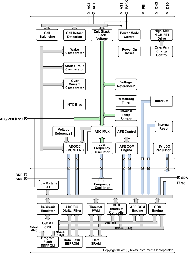
9.2 Functional Block Diagram
The Functional Block Diagram depicts the analog (AFE) and digital (AGG) peripheral content in the BQ28Z620 device.
