JAJSV55 August   2024 BQ2969

PRODUCTION DATA  

  1.   1
  2. 特長
  3. アプリケーション
  4. 概要
  5. Device Comparison Table
  6. Pin Configuration and Functions
  7. Specifications
    1. 6.1 Absolute Maximum Ratings
    2. 6.2 ESD Ratings
    3. 6.3 Recommended Operating Conditions
    4. 6.4 Thermal Information
    5. 6.5 Electrical Characteristics
    6. 6.6 Typical Characteristics
  8. Detailed Description
    1. 7.1 Overview
    2. 7.2 Functional Block Diagram
    3. 7.3 Feature Description
      1. 7.3.1 Pin Details
        1. 7.3.1.1 Input Sense Voltage, Vx
        2. 7.3.1.2 Output Drive, OUT
        3. 7.3.1.3 Supply Input, VDD
        4. 7.3.1.4 Regulated Supply Output, REG
      2. 7.3.2 Overvoltage Sensing for OUT
      3. 7.3.3 Regulator Output Voltage
    4. 7.4 Device Functional Modes
      1. 7.4.1 NORMAL Mode
      2. 7.4.2 OVERVOLTAGE Mode
      3. 7.4.3 UNDERVOLTAGE Mode
      4. 7.4.4 CUSTOMER TEST MODE
  9. Application and Implementation
    1. 8.1 Application Information
    2. 8.2 Typical Application
      1. 8.2.1 Design Requirements
      2. 8.2.2 Detailed Design Procedure
      3. 8.2.3 Application Curves
  10. Power Supply Recommendations
  11. 10Layout
    1. 10.1 Layout Guidelines
    2. 10.2 Layout Example
  12. 11Device and Documentation Support
    1. 11.1 サード・パーティ製品に関する免責事項
    2. 11.2 Receiving Notification of Documentation Updates
    3. 11.3 サポート・リソース
    4. 11.4 Trademarks
    5. 11.5 静電気放電に関する注意事項
    6. 11.6 用語集
  13. 12Revision History
  14. 13Mechanical, Packaging, and Orderable Information

パッケージ・オプション

メカニカル・データ(パッケージ|ピン)
サーマルパッド・メカニカル・データ
発注情報

Overvoltage Sensing for OUT

Each cell in the BQ2969 device is monitored independently for an overvoltage condition. Overvoltage is detected by comparing the actual cell voltage to a protection voltage reference, VOV. If any cell voltage exceeds the programmed VOV value, an internal timer circuit is activated. After the timer completes a fixed, pre-programmed delay, the OUT pin transitions from an inactive state to the active state.
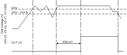
BQ2969 Timing for Overvoltage Sensing for OUTFigure 7-2 Timing for Overvoltage Sensing for OUT