JAJSV55 August 2024 BQ2969
PRODUCTION DATA
- 1
- 1 特長
- 2 アプリケーション
- 3 概要
- 4 Device Comparison Table
- 5 Pin Configuration and Functions
- 6 Specifications
- 7 Detailed Description
- 8 Application and Implementation
- 9 Power Supply Recommendations
- 10Layout
- 11Device and Documentation Support
- 12Revision History
- 13Mechanical, Packaging, and Orderable Information
パッケージ・オプション
メカニカル・データ(パッケージ|ピン)
- DSG|8
サーマルパッド・メカニカル・データ
- DSG|8
発注情報
8.2 Typical Application
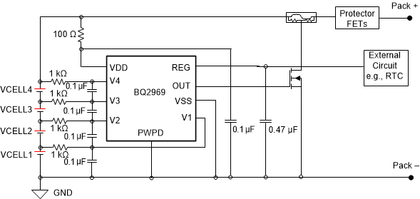
Figure 8-1 shows a simplified application schematic using the BQ2969 together with the associated passive components and external NFET to flow a high-side fuse.
 Figure 8-1 BQ2969
4-Series Cell Typical Implementation (Simplified Schematic)
 A full schematic of a basic circuit based on the BQ2969 for a 4-series battery pack evaluation module is shown below. Figure 10-1 and Figure 10-2 show the board layout for this design.
 Figure 8-2 BQ2969 4-Series Cell Schematic Diagram - Protector and
Fuse Blow Circuitry
 Figure 8-3 BQ2969 4-Series Cell Schematic Diagram - Cell Simulator
Circuitry