SBOS765 January 2016
PRODUCTION DATA.
10 Layout
10.1 Layout Guidelines
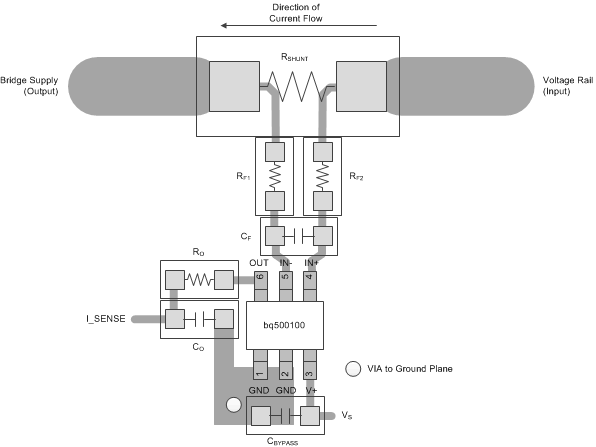
- Make connections to the shunt resistor with a Kelvin or 4-wire connection. This connection technique ensures that only the current-sensing resistor impedance is detected between the input pins. Poor routing of the current-sensing resistor commonly results in additional resistance present between the input pins. Given the very low ohmic value of the current resistor, any additional high-current carrying impedance can cause significant measurement errors.
- Place the power-supply bypass capacitor as closely as possible to the supply and ground pins. The recommended value of this bypass capacitor is 0.1 μF. Additional decoupling capacitance can be added to compensate for noisy or high-impedance power supplies.
- Place the input filter capacitor, CF, as close as possible to the input pins of the device. Place the input filter resistors as close as possible to each other to minimize the enclosed loop area between the device and the shunt resistor.
- The output of the current-sense circuit must be located as close as possible to the wireless power transmitter manager device. If the distance to the wireless power transmitter is greater than 1 cm, the output filter capacitor (CO) shown in Figure 8 must be placed next to the I_SENSE pin of the wireless power transmitter manger. Placing the capacitor at the I_SENSE pin of the wireless power transmitter manger provides the best filtering of the current-sense signal.
10.2 Layout Example
 Figure 8. Recommended Layout