SLPS585 March 2016
PRODUCTION DATA.
- 1 Features
- 2 Applications
- 3 Description
- 4 Revision History
- 5 Pin Configuration and Functions
- 6 Specifications
- 7 Detailed Description
- 8 Application and Implementation
- 9 Layout
- 10Device and Documentation Support
- 11Mechanical, Packaging, and Orderable Information
パッケージ・オプション
デバイスごとのパッケージ図は、PDF版データシートをご参照ください。
メカニカル・データ(パッケージ|ピン)
- DPC|8
サーマルパッド・メカニカル・データ
発注情報
7 Detailed Description
7.1 Overview
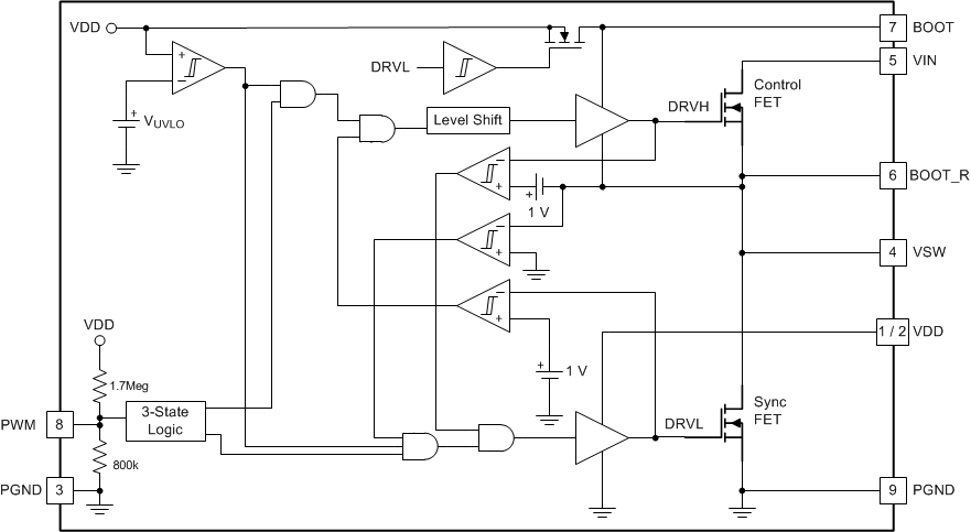
The bq500101 NexFET™ Power Stage is a highly optimized design for use in wireless power transmitter designs. The bq500101 can also be used for synchronous buck applications.
7.2 Functional Block Diagram

7.3 Feature Description
7.3.1 Powering bq500101 And Gate Drivers
An external VDD voltage is required to supply the integrated gate driver device and provide the necessary gate drive power for the MOSFETS. A 1-µF 10-V X5R or higher ceramic capacitor is recommended to bypass VDD pin to PGND. A bootstrap circuit to provide gate drive power for the Control FET is also included. The bootstrap supply to drive the Control FET is generated by connecting a 100-nF 16-V X5R ceramic capacitor CBOOT between BOOT and BOOT_R pins. An optional RBOOT resistor in series with CBOOT can be used to slow down the turn on speed of the Control FET and reduce voltage spikes on the VSW node. A typical 1 Ω to 4.7 Ω value is a compromise between switching loss and VSW spike amplitude.
7.3.2 Undervoltage Lockout Protection (UVLO)
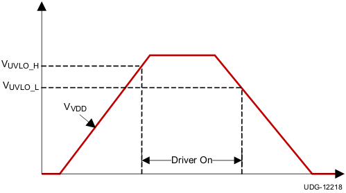
The undervoltage lockout (UVLO) comparator evaluates the VDD voltage level. As VVDD rises, both the Control FET and Sync FET gates hold actively low at all times until VVDD reaches the higher UVLO threshold (VUVLO_H)., Then the driver becomes operational and responds to PWM command. If VDD falls below the lower UVLO threshold (VUVLO_L = VUVLO_H – Hysteresis), the device disables the driver and drives the outputs of the Control FET and Sync FET gates actively low. Figure 1 shows this function.
 Figure 1. UVLO Operation
7.3.3 Integrated Boost-Switch
To maintain a BOOT-VSW voltage close to VDD (to get lower conduction losses on the high-side FET), the conventional diode between the VDD pin and the BOOT pin is replaced by a FET which is gated by the DRVL signal.