JAJSS72 November   2023 BQ76907

PRODUCTION DATA  

  1.   1
  2. 特長
  3. アプリケーション
  4. 概要
  5. Device Comparison Table
  6. Pin Configuration and Functions
  7. Specifications
    1. 6.1  Absolute Maximum Ratings
    2. 6.2  ESD Ratings
    3. 6.3  Recommended Operating Conditions
    4. 6.4  Thermal Information bq76907
    5. 6.5  Supply Current
    6. 6.6  Digital I/O
    7. 6.7  REGOUT LDO
    8. 6.8  Voltage References
    9. 6.9  Coulomb Counter
    10. 6.10 Coulomb Counter Digital Filter
    11. 6.11 Current Wake Detector
    12. 6.12 Analog-to-Digital Converter
    13. 6.13 Cell Balancing
    14. 6.14 Internal Temperature Sensor
    15. 6.15 Thermistor Measurement
    16. 6.16 Hardware Overtemperature Detector
    17. 6.17 Internal Oscillator
    18. 6.18 Charge and Discharge FET Drivers
    19. 6.19 Comparator-Based Protection Subsystem
    20. 6.20 Timing Requirements - I2C Interface, 100kHz Mode
    21. 6.21 Timing Requirements - I2C Interface, 400kHz Mode
    22. 6.22 Timing Diagram
    23. 6.23 Typical Characteristics
  8. Detailed Description
    1. 7.1 Overview
    2. 7.2 Functional Block Diagram
    3. 7.3 Device Configuration
      1. 7.3.1 Commands and Subcommands
      2. 7.3.2 Configuration Using OTP or Registers
      3. 7.3.3 Device Security
    4. 7.4 Device Hardware Features
      1. 7.4.1  Voltage ADC
      2. 7.4.2  Coulomb Counter and Digital Filters
      3. 7.4.3  Protection FET Drivers
      4. 7.4.4  Voltage References
      5. 7.4.5  Multiplexer
      6. 7.4.6  LDOs
      7. 7.4.7  Standalone Versus Host Interface
      8. 7.4.8  ALERT Pin Operation
      9. 7.4.9  Low Frequency Oscillator
      10. 7.4.10 I2C Serial Communications Interface
    5. 7.5 Measurement Subsystem
      1. 7.5.1 Voltage Measurement
        1. 7.5.1.1 Voltage ADC Scheduling
        2. 7.5.1.2 Unused VC Pins
        3. 7.5.1.3 General Purpose ADCIN Functionality
      2. 7.5.2 Current Measurement and Charge Integration
      3. 7.5.3 Internal Temperature Measurement
      4. 7.5.4 Thermistor Temperature Measurement
      5. 7.5.5 Factory Trim and Calibration
    6. 7.6 Protection Subsystem
      1. 7.6.1 Protections Overview
      2. 7.6.2 Primary Protections
      3. 7.6.3 CHG Detector
      4. 7.6.4 Cell Open-Wire Protection
      5. 7.6.5 Diagnostic Checks
    7. 7.7 Cell Balancing
    8. 7.8 Device Operational Modes
      1. 7.8.1 Overview of Operational Modes
      2. 7.8.2 NORMAL Mode
      3. 7.8.3 SLEEP Mode
      4. 7.8.4 DEEPSLEEP Mode
      5. 7.8.5 SHUTDOWN Mode
      6. 7.8.6 CONFIG_UPDATE Mode
  9. Application and Implementation
    1. 8.1 Application Information
    2. 8.2 Typical Application
      1. 8.2.1 Design Requirements
      2. 8.2.2 Detailed Design Procedure
      3. 8.2.3 Application Performance Plot
      4. 8.2.4 Random Cell Connection Support
      5. 8.2.5 Startup Timing
      6. 8.2.6 FET Driver Turn-Off
      7. 8.2.7 Usage of Unused Pins
  10. Power Supply Recommendations
  11. 10Layout
    1. 10.1 Layout Guidelines
    2. 10.2 Layout Example
  12. 11Device and Documentation Support
    1. 11.1 Documentation Support
      1. 11.1.1 Related Documentation
    2. 11.2 ドキュメントの更新通知を受け取る方法
    3. 11.3 サポート・リソース
    4. 11.4 Trademarks
    5. 11.5 静電気放電に関する注意事項
    6. 11.6 用語集
  13. 12Revision History
  14. 13Introduction to Mechanical, Packaging, and Orderable Information

パッケージ・オプション

メカニカル・データ(パッケージ|ピン)
サーマルパッド・メカニカル・データ
発注情報

Typical Characteristics

GUID-20231009-SS0I-ZDZW-NFQ7-Z3S0ZXCLDSRV-low.svg
Figure 6-2 Cell Voltage Measurement Error at 25°C Across Input Range
GUID-20231009-SS0I-LT5P-L9JR-RKDXL9TDG9CV-low.svg
Figure 6-4 Cell Voltage Measurement Error vs. Temperature with Cell Voltage = 1.0 V
GUID-20231009-SS0I-NWZS-32CR-ND1CPLCWBPN0-low.svg
Figure 6-6 Cell Voltage Measurement Error vs. Temperature with Cell Voltage = 2.0 V
GUID-20231009-SS0I-PTZX-6TQR-SZLPMW0JVLHF-low.svg
Figure 6-8 Cell Voltage Measurement Error vs. Temperature with Cell Voltage = 3.0 V
GUID-20231009-SS0I-QKWJ-TRVF-0J2FXHXW85VT-low.svg
Figure 6-10 Cell Voltage Measurement Error vs. Temperature with Cell Voltage = 4.0 V
GUID-20231009-SS0I-HHST-GFDQ-Z1HHGMCBZKFV-low.svg
Figure 6-12 Cell Voltage Measurement Error vs. Temperature with Cell Voltage = 5.0 V
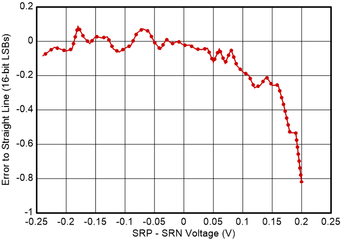
GUID-20231012-SS0I-8979-9P6G-SZTFCDWQ3R1V-low.png
Figure 6-14 Current Linearity Error vs. Sense Resistor Voltage
GUID-20231009-SS0I-VJJ4-JSRZ-PKMKQWJJ3DZM-low.svg
Figure 6-16 Internal Temperature Measurement Raw Codes vs. Temperature
GUID-20231009-SS0I-FNMQ-KS1K-NTHXNTX6WFW0-low.svg
Figure 6-18 Thermistor Pullup Resistance vs. Temperature
GUID-20231011-SS0I-JNDP-VBBS-KGCDWNGQ5STS-low.svg
Figure 6-20 Overcurrent in Discharge Protection 1 (OCD1) Threshold vs. Temperature
GUID-20231011-SS0I-1LNR-VXZM-JGH3XVGB8CGG-low.svg
Figure 6-22 Short Circuit in Discharge Protection (SCD) Threshold vs. Temperature
GUID-20231011-SS0I-ZPKF-QBVZ-1SJWNQKXGQSN-low.svg
Figure 6-24 REGOUT Voltage vs. Temperature and Load
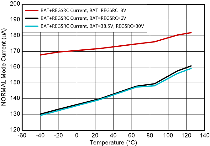
GUID-20231012-SS0I-WHXZ-VFZZ-R1ZZRRL0QS7Q-low.png
When REGSRC = 3 V, REGSRC current increases as the device attempts to raise the REGOUT voltage to its target 3.3 V.
Figure 6-26 Supply Current in NORMAL Mode vs. Temperature
GUID-20231012-SS0I-PCM5-GPZJ-NPCZDLWW6T1F-low.svg
Figure 6-28 Supply Current in DEEPSLEEP Mode vs. Temperature
GUID-20231009-SS0I-S49Q-2F14-HRJWKGS99GZF-low.svg
Figure 6-3 Cell Voltage Measurement Error vs. Temperature with Cell Voltage = 0.5 V
GUID-20231009-SS0I-SBNX-JZ8F-2NCVHJFD4LDB-low.svg
Figure 6-5 Cell Voltage Measurement Error vs. Temperature with Cell Voltage = 1.5 V
GUID-20231009-SS0I-DBZP-QT4F-4L9KQQMHNXSB-low.svg
Figure 6-7 Cell Voltage Measurement Error vs. Temperature with Cell Voltage = 2.5 V
GUID-20231009-SS0I-4RZH-X8LB-QJGP7JF5DGSH-low.svg
Figure 6-9 Cell Voltage Measurement Error vs. Temperature with Cell Voltage = 3.5 V
GUID-20231009-SS0I-XMTF-XTL9-LGRFBQFBMN7S-low.svg
Figure 6-11 Cell Voltage Measurement Error vs. Temperature with Cell Voltage = 4.5 V
GUID-20231009-SS0I-WNBK-CKPL-GF4HQ4JH997D-low.svg
Figure 6-13 Cell Voltage Measurement Error vs. Temperature with Cell Voltage = 5.5 V
GUID-20231009-SS0I-02XQ-CM8P-7N2XTZW6DSBB-low.svg
Figure 6-15 Internal Voltage References vs. Temperature (VREF1 and VREF2)
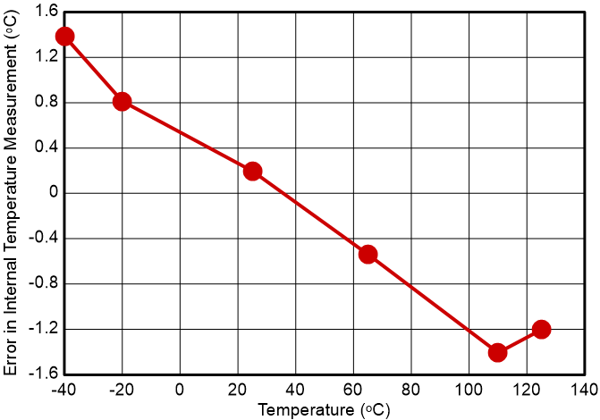
GUID-B112C7C7-D7F0-4E55-B3EE-F6A1D98F9826-low.png
Figure 6-17 Internal Temperature Measurement Error vs. Temperature
GUID-20231009-SS0I-LS80-BLGX-BMRWKMDGNQVS-low.svg
LFO measured in full speed mode (262 kHz) and low speed mode (32.77 kHz)
Figure 6-19 Low Frequency Oscillator (LFO) Accuracy vs. Temperature
GUID-20231011-SS0I-99WV-MPHB-F4BTFKGKDQJF-low.svg
Figure 6-21 Overcurrent in Charge Protection (OCC) Threshold vs. Temperature
GUID-20231011-SS0I-S3JV-HG7W-XXMHXQPCJQNX-low.svg
Data is collected with a 1.5-V differential input on cell.
Figure 6-23 Cell Balancing Resistance vs. Temperature
GUID-20231011-SS0I-Q9NX-CPS2-VHWXXCVQFFZK-low.svg
Figure 6-25 TS and VC0 Wake Voltage vs. Temperature
GUID-20231012-SS0I-6TPS-Z0L0-WZHPX88VZFTP-low.svg
No communications, REGOUT disabled
Figure 6-27 Supply Current in SLEEP Mode vs. Temperature
GUID-20231012-SS0I-RRQL-P3WD-FW7VV4XXZQZ9-low.svg
Figure 6-29 Supply Current in SHUTDOWN Mode vs. Temperature