JAJSSH0 December 2023 BQ77307
PRODUCTION DATA
- 1
- 1 特長
- 2 アプリケーション
- 3 概要
- 4 Device Comparison Table
- 5 Pin Configuration and Functions
-
6 Specifications
- 6.1 Absolute Maximum Ratings
- 6.2 ESD Ratings
- 6.3 Recommended Operating Conditions
- 6.4 Thermal Information BQ77307
- 6.5 Supply Current
- 6.6 Digital I/O
- 6.7 REGOUT LDO
- 6.8 Voltage References
- 6.9 Current Detector
- 6.10 Thermistor Pullup Resistor
- 6.11 Hardware Overtemperature Detector
- 6.12 Internal Oscillator
- 6.13 Charge and Discharge FET Drivers
- 6.14 Protection Subsystem
- 6.15 Timing Requirements - I2C Interface, 100kHz Mode
- 6.16 Timing Requirements - I2C Interface, 400kHz Mode
- 6.17 Timing Diagram
- 6.18 Typical Characteristics
-
7 Detailed Description
- 7.1 Overview
- 7.2 Functional Block Diagram
- 7.3 Device Configuration
- 7.4
Device Hardware Features
- 7.4.1 Voltage Protection Subsystem
- 7.4.2 Current Protection Subsystem
- 7.4.3 Unused VC Pins
- 7.4.4 Internal Temperature Protection
- 7.4.5 Thermistor Temperature Protections
- 7.4.6 Protection FET Drivers
- 7.4.7 Voltage References
- 7.4.8 Multiplexer
- 7.4.9 LDOs
- 7.4.10 Standalone Versus Host Interface
- 7.4.11 ALERT Pin Operation
- 7.4.12 Low Frequency Oscillator
- 7.4.13 I2C Serial Communications Interface
- 7.5 Protection Subsystem
- 7.6 Device Power Modes
- 8 Application and Implementation
- 9 Power Supply Recommendations
- 10Layout
- 11Device and Documentation Support
- 12Revision History
- 13Mechanical, Packaging, and Orderable Information
パッケージ・オプション
メカニカル・データ(パッケージ|ピン)
- RGR|20
サーマルパッド・メカニカル・データ
- RGR|20
発注情報
8.2 Typical Application
A simplified application schematic for a 7-series battery pack is shown in BQ77307 7-Series Cell Typical Implementation (Simplified Schematic), using the BQ77307 as a primary protector together with a host microcontroller and a communications transceiver. This configuration uses low-side CHG and DSG FETs in series. Several points to consider in an implementation are included below:
- A series diode is recommended at the BAT pin, together with a capacitor from the pin to VSS. These components allow the device to continue operating for a short time when a pack short circuit occurs, which may cause the top-of-stack voltage to drop to approximately 0 V. In this case, the diode prevents the BAT pin from being pulled low with the stack, and the device will continue to operate, drawing current from the capacitor. Generally, operation is only required for a short time until the device detects the short circuit event and disables the DSG FET. A Schottky diode can be used if low voltage pack operation is needed, or a conventional diode can be used otherwise.
- The FET CHG and DSG drivers use the REGSRC pin for their supply, so the user may also prefer to include a diode between the top of the stack and the REGSRC pin, similar to that used for the BAT pin. If any resistance (> 1 Ω) is included in series between the top of the stack and the REGSRC pin, it is recommended to include a 1 μF capacitor at the REGSRC pin to VSS. The REGSRC pin can be shorted to the BAT pin and a single diode used, but this may result in the BAT pin voltage dropping more rapidly during a short circuit event due to the increased loading of the REGOUT regulator drawing from the REGSRC pin.
- The recommended minimum voltage on the VC0 to VC4 pins extends down to –0.2 V, while the recommended minimum voltage on the VC5, VC6, and VC7 pins is limited to 2.0 V, relative to VSS. This restriction exists to ensure the specified accuracy of cell voltage protections.
- TI recommends using 100-Ω resistors in series with the SRP and SRN pins, and a 100 nF with optional 100-pF differential filter capacitance between the pins for filtering. The routing of these components, together with the sense resistor, to the pins should be minimized and fully symmetric, with all components recommended to stay on the same side of the PCB with the device. Capacitors connected from the pins to VSS can provide filtering of common mode transients from reaching the pins, but they may also have a slight impact on current protection performance.
- The filter network connected between the sense resistor and the SRP and SRN pins introduces an analog filter delay that can be important when fast current protections are required, such as in determining the short circuit in discharge (SCD) time until FETs are disabled. If the delay introduced by this network is too long, the resistance and capacitance values can be reduced. This will have a tradeoff of providing less analog filtering of high-frequency components.
- Due to thermistors often being attached to cells and possibly needing long wires to connect back to the device, it may be helpful to add a capacitor from the thermistor pin to the device VSS. However, it is important to not use too large of a value of capacitor, since this will affect the settling time when the thermistor is biased and checked periodically. It is recommended to keep the value of external capacitance below 7.5 nF.

Figure 8-1 BQ77307 7-Series Cell Typical Implementation (Simplified Schematic)
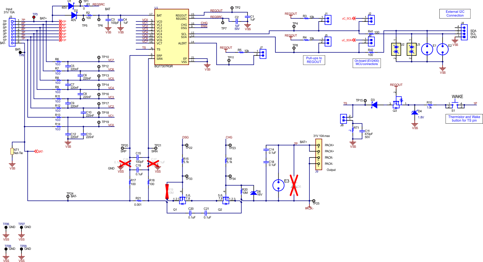
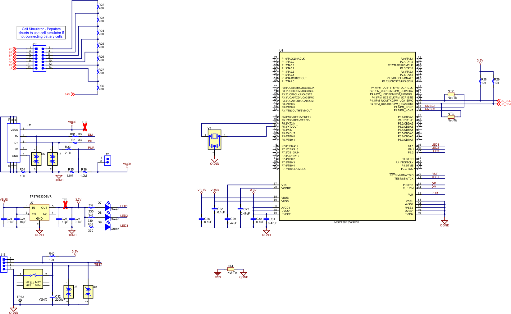
A full schematic of a basic monitor circuit based on the BQ77307 for a 7-series battery pack is shown below. Section 10.2 shows the board layout for this design.
 Figure 8-2 BQ77307 7-Series Cell Schematic Diagram—Monitor
 Figure 8-3 BQ77307 7-Series Cell Schematic Diagram—Additional Circuitry