JAJSSH0 December 2023 BQ77307
PRODUCTION DATA
- 1
- 1 特長
- 2 アプリケーション
- 3 概要
- 4 Device Comparison Table
- 5 Pin Configuration and Functions
-
6 Specifications
- 6.1 Absolute Maximum Ratings
- 6.2 ESD Ratings
- 6.3 Recommended Operating Conditions
- 6.4 Thermal Information BQ77307
- 6.5 Supply Current
- 6.6 Digital I/O
- 6.7 REGOUT LDO
- 6.8 Voltage References
- 6.9 Current Detector
- 6.10 Thermistor Pullup Resistor
- 6.11 Hardware Overtemperature Detector
- 6.12 Internal Oscillator
- 6.13 Charge and Discharge FET Drivers
- 6.14 Protection Subsystem
- 6.15 Timing Requirements - I2C Interface, 100kHz Mode
- 6.16 Timing Requirements - I2C Interface, 400kHz Mode
- 6.17 Timing Diagram
- 6.18 Typical Characteristics
-
7 Detailed Description
- 7.1 Overview
- 7.2 Functional Block Diagram
- 7.3 Device Configuration
- 7.4
Device Hardware Features
- 7.4.1 Voltage Protection Subsystem
- 7.4.2 Current Protection Subsystem
- 7.4.3 Unused VC Pins
- 7.4.4 Internal Temperature Protection
- 7.4.5 Thermistor Temperature Protections
- 7.4.6 Protection FET Drivers
- 7.4.7 Voltage References
- 7.4.8 Multiplexer
- 7.4.9 LDOs
- 7.4.10 Standalone Versus Host Interface
- 7.4.11 ALERT Pin Operation
- 7.4.12 Low Frequency Oscillator
- 7.4.13 I2C Serial Communications Interface
- 7.5 Protection Subsystem
- 7.6 Device Power Modes
- 8 Application and Implementation
- 9 Power Supply Recommendations
- 10Layout
- 11Device and Documentation Support
- 12Revision History
- 13Mechanical, Packaging, and Orderable Information
パッケージ・オプション
メカニカル・データ(パッケージ|ピン)
- RGR|20
サーマルパッド・メカニカル・データ
- RGR|20
発注情報
8.2.3 Application Performance Plot
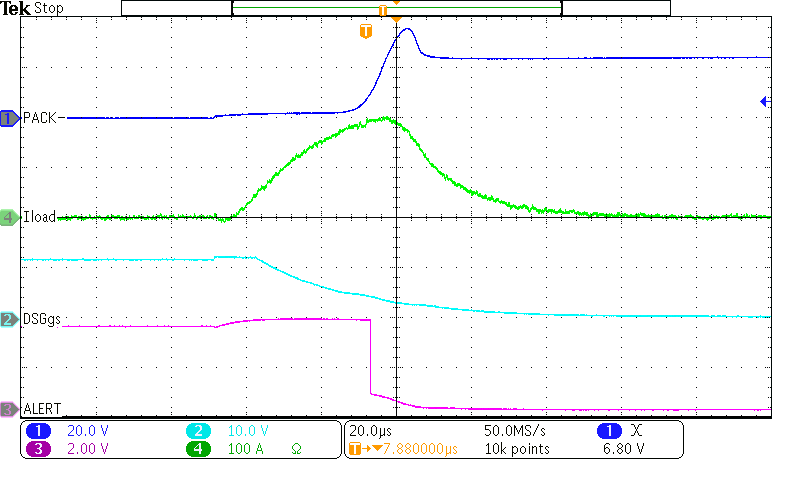
The scope plot example below shows the response of the device to a short circuit in discharge (SCD) event and subsequent protection. The device example is configured with an SCD threshold = 10 mV and SCD delay of 0 μs to 15 μs. A short circuit is applied through a 1-mΩ sense resistor. The input filter network on the SRP and SRN pins consists of 100-Ω resistors and a 100-nF differential capacitor, which results in a 20-μs time constant. The [SSA] bit in AlarmStatus() causes the ALERT pin to fall, which occurs between approximately 15 μs and 30 μs after the safety status is triggered and the DSG driver is disabled. The circuit includes a 5.1-kΩ resistor between the DSG pin and the DSG FET gate. The load current is shown using the differential voltage at the SRN-SRP pins, which includes an RC delay versus the voltage at the sense resistor
 Figure 8-4 Scope
Plot
of SCD
Event
and
Protection