JAJSCB2K April 2020 – July 2020 BQ77904 , BQ77905
PRODUCTION DATA
- 1 特長
- 2 アプリケーション
- 3 概要
- 4 Revision History
- 5 Device Comparison
- 6 Pin Configuration and Functions
- 7 Specifications
-
8 Detailed Description
- 8.1 Overview
- 8.2 Functional Block Diagram
- 8.3
Feature Description
- 8.3.1 Protection Summary
- 8.3.2
Fault Operation
- 8.3.2.1 Operation in OV
- 8.3.2.2 Operation in UV
- 8.3.2.3 Operation in OW
- 8.3.2.4 Operation in OCD1
- 8.3.2.5 Operation in OCD2
- 8.3.2.6 Operation in SCD
- 8.3.2.7 Overcurrent Recovery Timer
- 8.3.2.8 Load Removal Detection
- 8.3.2.9 Load Removal Detection in UV
- 8.3.2.10 Operation in OTC
- 8.3.2.11 Operation in OTD
- 8.3.2.12 Operation in UTC
- 8.3.2.13 Operation in UTD
- 8.3.3 Protection Response and Recovery Summary
- 8.3.4 Configuration CRC Check and Comparator Built-In-Self-Test
- 8.3.5 Fault Detection Method
- 8.3.6 State Comparator
- 8.3.7 DSG FET Driver Operation
- 8.3.8 CHG FET Driver Operation
- 8.3.9 External Override of CHG and DSG Drivers
- 8.3.10 Configuring 3-S, 4-S, or 5-S Mode
- 8.3.11 Stacking Implementations
- 8.3.12 Zero-Volt Battery Charging Inhibition
- 8.4 Device Functional Modes
- 9 Application and Implementation
- 10Power Supply Recommendations
- 11Layout
- 12Device and Documentation Support
- 13Mechanical, Packaging, and Orderable Information
9.1.1.1 CHG and DSG FET Rise and Fall Time
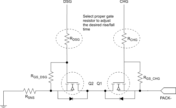
The CHG and DSG FET drivers are designed to have fast switching time. Users should select a proper gate resistor (RCHG and RDSG in the reference schematic) to set to the desired rise/fall time.
 Figure 9-1 Select Proper Gate Resistor for FET Rise and Fall Time
The CHG FET fall time is generally slower, because it is connected to the PACK– terminal. The CHG driver will pull to VSS quickly when the driver is signaled to turn off. Once the gate of the CHG FET reaches ground or Vgsth, the PACK– will start to fall below ground and the CHG signal will follow suit in order to turn off the CHG FET. This portion of the fall time is strongly dependent on the FET characteristic, the number of FETs in parallel, and the value of gate-source resistor (RGS_CHG).
 Figure 9-2 CHG FET Fall Time