JAJSCB2K April 2020 – July 2020 BQ77904 , BQ77905
PRODUCTION DATA
- 1 特長
- 2 アプリケーション
- 3 概要
- 4 Revision History
- 5 Device Comparison
- 6 Pin Configuration and Functions
- 7 Specifications
-
8 Detailed Description
- 8.1 Overview
- 8.2 Functional Block Diagram
- 8.3
Feature Description
- 8.3.1 Protection Summary
- 8.3.2
Fault Operation
- 8.3.2.1 Operation in OV
- 8.3.2.2 Operation in UV
- 8.3.2.3 Operation in OW
- 8.3.2.4 Operation in OCD1
- 8.3.2.5 Operation in OCD2
- 8.3.2.6 Operation in SCD
- 8.3.2.7 Overcurrent Recovery Timer
- 8.3.2.8 Load Removal Detection
- 8.3.2.9 Load Removal Detection in UV
- 8.3.2.10 Operation in OTC
- 8.3.2.11 Operation in OTD
- 8.3.2.12 Operation in UTC
- 8.3.2.13 Operation in UTD
- 8.3.3 Protection Response and Recovery Summary
- 8.3.4 Configuration CRC Check and Comparator Built-In-Self-Test
- 8.3.5 Fault Detection Method
- 8.3.6 State Comparator
- 8.3.7 DSG FET Driver Operation
- 8.3.8 CHG FET Driver Operation
- 8.3.9 External Override of CHG and DSG Drivers
- 8.3.10 Configuring 3-S, 4-S, or 5-S Mode
- 8.3.11 Stacking Implementations
- 8.3.12 Zero-Volt Battery Charging Inhibition
- 8.4 Device Functional Modes
- 9 Application and Implementation
- 10Power Supply Recommendations
- 11Layout
- 12Device and Documentation Support
- 13Mechanical, Packaging, and Orderable Information
9.1.1.4 Using Load Detect for UV Fault Recovery
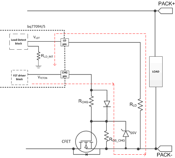
A larger CHG FET gate-source resistor is required if load removal is enabled as part of the UV recovery criteria. When the load removal circuit is enabled, the device is internally connected to Vss. Because in a UV fault the CHG driver remains on, it creates a resistor divider path to the load detect circuit.
 Figure 9-6 Load Detect Circuit During UV Fault
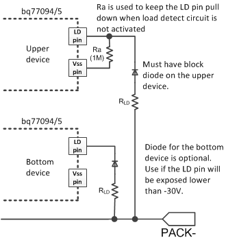
To ensure load removal is detected properly during a UV fault, TI recommends to use 3.3 MΩ for RGS_CHG (instead of a typical of 1 MΩ when load removal is NOT required for UV recovery). RCHG can stay in 1 MΩ as recommended when using CHG FET protection components. The CHG FET rise time impact is minimized as described in the Protecting CHG FET section. On a stacked configuration, connect the LD pin, as shown in Figure 9-7 if load removal is used for a UV fault recovery. If load detection is not required for a UV fault recovery, a larger value of RGS_CHG can be used (that is, 10 MΩ) and the LD pin on the upper devices can be left floating.
 Figure 9-7 Simplified Circuit: LD Connection on Upper Device When Using for UV Fault Recovery