JAJSEZ9L march 2018 – august 2023 BQ77915
PRODUCTION DATA
- 1
- 1 特長
- 2 アプリケーション
- 3 概要
- 4 Revision History
- 5 概要 (続き)
- 6 Device Comparison Table
- 7 Pin Configuration and Functions
- 8 Specifications
-
9 Detailed Description
- 9.1 Overview
- 9.2 Functional Block Diagram
- 9.3
Feature Description
- 9.3.1 Protection Summary
- 9.3.2
Fault Operation
- 9.3.2.1 Operation in OV
- 9.3.2.2 Operation in UV
- 9.3.2.3 Operation in OW
- 9.3.2.4 Operation in OCD1
- 9.3.2.5 Operation in OCD2
- 9.3.2.6 Programming the OCD1/2 Delay Using the OCDP Pin
- 9.3.2.7 Operation in SCD
- 9.3.2.8 Operation in OCC
- 9.3.2.9 Overcurrent Recovery Timer
- 9.3.2.10 Load Detection and Load Removal Detection
- 9.3.2.11 Operation in OTC
- 9.3.2.12 Operation in OTD
- 9.3.2.13 Operation in UTC
- 9.3.2.14 Operation in UTD
- 9.3.3 Protection Response and Recovery Summary
- 9.3.4 Cell Balancing
- 9.3.5 HIBERNATE Mode Operation
- 9.3.6 Configuration CRC Check and Comparator Built-In-Self-Test
- 9.3.7 Fault Detection Method
- 9.3.8 State Comparator
- 9.3.9 DSG FET Driver Operation
- 9.3.10 CHG FET Driver Operation
- 9.3.11 External Override of CHG and DSG Drivers
- 9.3.12 Configuring 3-Series, 4-Series, or 5-Series Modes
- 9.3.13 Stacking Implementations
- 9.3.14 Zero-Volt Battery Charging Inhibition
- 9.4 Device Functional Modes
-
10Application and Implementation
- 10.1
Application Information
- 10.1.1 Recommended System Implementation
- 10.2 Typical Application
- 10.1
Application Information
- 11Power Supply Recommendations
- 12Layout
- 13Device and Documentation Support
- 14Mechanical, Packaging, and Orderable Information
9.3.4 Cell Balancing
Cell balancing is performed by comparing the cell voltages with respect to cell balancing threshold voltages, evaluating the results of the comparison and controlling the cell balancing FET, which over a period of time will allow for closer cell voltages, thereby extending battery pack life. The conditions for performing cell balancing are: CBI is connected to VSS, no device in the stack is in a fault condition, and the pack is charging. The State Comparator section lists the conditions for the device's charging state.
CBI is the cell balancing input pin. It enables cell balancing function for the device.
- Leave the CBI pin floating to disable cell balancing. An internal circuit pulls up the CBI pin to AVDD in this case.
- Connect CBI to VSS to enable cell balancing.
In a single device, cell balancing of all the odd numbered cells can happen at the same time, and balancing of all the even numbered cells can also happen at the same time, but odd and even cells are not balanced at the same time. When devices are stacked on top of each other, verify in the PCB layout that the trace from VC5 pin to a cell and the trace from the VC0 pin of the next upper device to the immediately higher cell are kept separate.
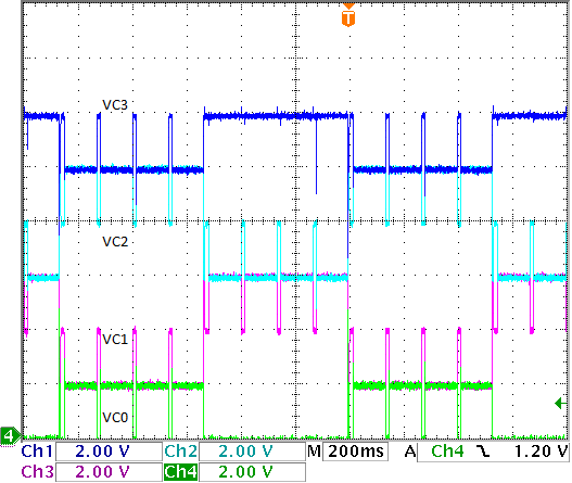
All cell balancing FETs are turned off during voltage measurements. If odd numbered and even numbered cells need balancing at the same time, one single cycle time tBAL is dedicated for odd numbered cells alone followed by the next tBAL dedicated for even numbered cells alone. See an example of adjacent cell balancing in Figure 9-1.
 Figure 9-1 Balancing
Cells
1, 2, and 3
Figure 9-1 Balancing
Cells
1, 2, and 3In a stacked configuration, the CBO pin of the bottom device must be connected to the CBI pin of the next upper device through a 10-kΩ resistor and so forth.
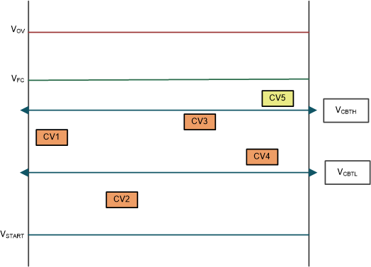
When a cell is in OV, its corresponding balancing FET is turned on if CBI is connected to VSS and if there are no discharge faults anywhere in the stack. The balancing FET is ON until the cell voltage drops to VFC or VOV – VHYS_OV, whichever occurs earlier.
 Figure 9-2 Cell-Balancing Algorithm
VCBTL is the lower cell balancing threshold and VCBTH is the upper cell balancing threshold. In Figure 9-2, the balancing FET is turned on only for the cell CV5. The BQ77915 VSTART is set at 3.8 V; therefore, cell balancing starts only when individual cell voltages exceed 3.8 V. The difference between VCBTH and VCBTL can be programmed in the EEPROM to be between 50 mV and 200 mV, in steps of 50 mV. The difference between the VOV and VFC can also be programmed in the EEPROM to be between 50 mV and 200 mV, in steps of 50 mV.
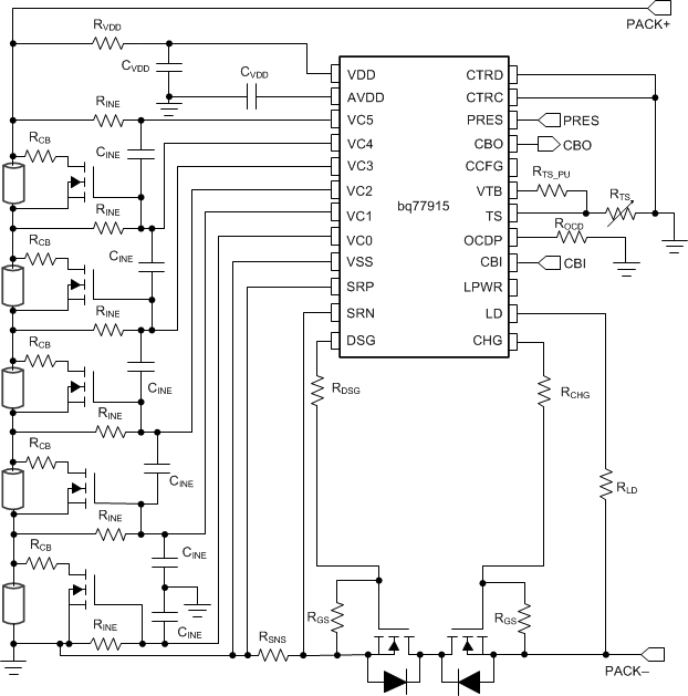
When using the integrated MOSFETs for cell balancing, the cell monitor filter resistance RINI controls the amount of cell balancing current the device can supply to the cells. Internal cell balancing should be used for cell balancing currents up to 50 mA. External MOSFETs have to be used if higher cell balancing currents are required. In the case of external balancing, the balancing current is controlled by the resistor RCB in series with the external MOSFET, as shown in Figure 9-3. The pin filter resistance RINE should be 1 kΩ and the capacitance CINE should be 0.1 µF. The gate bias voltage necessary to turn on the FET connected to Cell(n) is generated by the resistor RINE connected to the VC(n–1) pin. The external MOSFET must be selected with a threshold voltage less than 1.7 V.
 Figure 9-3 Cell Balancing with External MOSFETs