JAJSMA5C June   2021  – March 2022 BUF802

PRODUCTION DATA  

  1. 特長
  2. アプリケーション
  3. 説明
  4. Revision History
  5. Pin Configuration and Functions
  6. Specifications
    1. 6.1 Absolute Maximum Ratings
    2. 6.2 ESD Ratings
    3. 6.3 Recommended Operating Conditions
    4. 6.4 Thermal Information
    5. 6.5 Electrical Characteristics: Wide Bandwidth Mode
    6. 6.6 Electrical Characteristics: Low Quiescent Current Mode
    7. 6.7 Typical Characteristics
  7. Parameter Measurement Information
  8. Detailed Description
    1. 8.1 Overview
    2. 8.2 Functional Block Diagram
    3. 8.3 Feature Description
      1. 8.3.1 Input and Output Over-Voltage Clamp
      2. 8.3.2 Adjustable Quiescent Current
      3. 8.3.3 ESD Structure
    4. 8.4 Device Functional Modes
      1. 8.4.1 Buffer Mode (BF Mode)
      2. 8.4.2 Composite Loop Mode (CL Mode)
  9. Application and Implementation
    1. 9.1 Application Information
    2. 9.2 Typical Application
      1. 9.2.1 Oscilloscope Front-End Amplifier Design
        1. 9.2.1.1 Design Requirements
        2. 9.2.1.2 Detailed Design Procedure
        3. 9.2.1.3 Application Curves
      2. 9.2.2 Transforming a Wide-Bandwidth, 50 Ω Input Signal Chain to High-Input Impedance
        1. 9.2.2.1 Detailed Design Results
        2. 9.2.2.2 Application Curves
  10. 10Power Supply Recommendations
  11. 11Layout
    1. 11.1 Layout Guidelines
    2. 11.2 Layout Example
  12. 12Device and Documentation Support
    1. 12.1 Documentation Support
      1. 12.1.1 Related Documentation
    2. 12.2 Receiving Notification of Documentation Updates
    3. 12.3 サポート・リソース
    4. 12.4 Trademarks
    5. 12.5 Electrostatic Discharge Caution
    6. 12.6 Glossary
  13. 13Mechanical, Packaging, and Orderable Information

パッケージ・オプション

メカニカル・データ(パッケージ|ピン)
サーマルパッド・メカニカル・データ
発注情報

Parameter Measurement Information

Figure 7-1 through Figure 7-3 show the various test setup configurations for the BUF802.

Figure 7-1 Main Path Electrical Characteristics Measurement
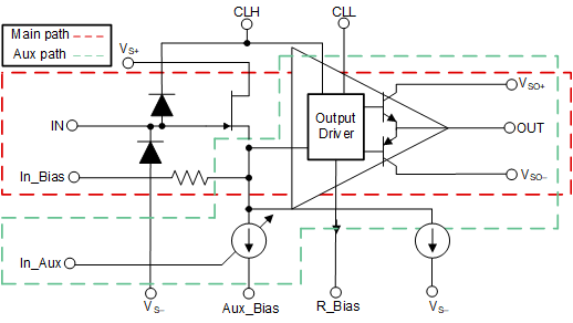
GUID-20210216-CA0I-VSPM-NLZ5-QT7GGP7C67HN-low.gifFigure 7-2 Main Path and Auxiliary Path
GUID-20210213-CA0I-NWTL-H8M8-RCXVBLM9M8C3-low.gifFigure 7-3 Auxiliary Path Electrical Characteristics Measurement

Figure 7-2 shows the two inputs for BUF802 (IN and In_Aux) which control the output. The IN pin controls the output of BUF802 through the Main Path, whereas the In_Aux pin controls the output through the Auxiliary Path. Either the Main Path or the Auxiliary Path, can be used to steer the output. The electrical characteristics of the Main Path and the Auxiliary Path is specified in Section 6.7.