JAJSMA5C June 2021 – March 2022 BUF802
PRODUCTION DATA
- 1 特長
- 2 アプリケーション
- 3 説明
- 4 Revision History
- 5 Pin Configuration and Functions
- 6 Specifications
- 7 Parameter Measurement Information
- 8 Detailed Description
- 9 Application and Implementation
- 10Power Supply Recommendations
- 11Layout
- 12Device and Documentation Support
- 13Mechanical, Packaging, and Orderable Information
パッケージ・オプション
メカニカル・データ(パッケージ|ピン)
- RGT|16
サーマルパッド・メカニカル・データ
- RGT|16
発注情報
5 Pin Configuration and Functions
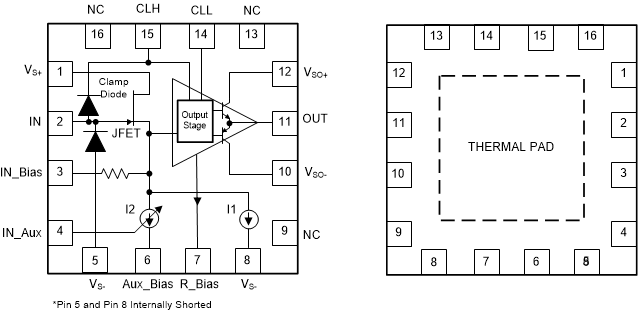
 Figure 5-1 RGT Package, 16-Pin VQFN
(Top View and Bottom View)
Table 5-1 Pin Functions
| PIN | TYPE(4) | Operating Mode(1)(2) | DESCRIPTION | |
|---|---|---|---|---|
| NAME | NO. | |||
| Aux_Bias | 6 | P | CL | Connect to VS- to enable control of OUT through the In_Aux. |
| CLH | 15 | I | BF, CL | Input pin for setting positive clamp voltage |
| CLL | 14 | I | BF, CL | Input pin for setting negative clamp voltage |
| IN | 2 | I | BF, CL | Signal input |
| In_Aux | 4 | I | CL | Auxiliary input for controlling OUT through an external amplifier. |
| In_Bias | 3 | I | CL | JFET biasing pin |
| NC | 16, 13, 9 | — | — | Do not connect. |
| OUT | 11 | O | BF, CL | Signal output |
| R_Bias | 7 | I | BF, CL | Output stage bias current setting pin |
| VS+ | 1 | P | BF, CL | Positive power supply connection for Input Stage. |
| VS- | 5, 8 | P | BF, CL | Negative power supply connection for Input Stage. Pin 5 and Pin 8 are internally shorted. |
| VSO+(3) | 12 | P | BF, CL | Positive power supply connection for Output Stage. |
| VSO-(3) | 10 | P | BF, CL | Negative power supply connection for Output Stage. |
| Thermal Pad | — | — | The thermal pad is electrically isolated from the die and pins. Connect the thermal pad to any potential. | |
(1) See Section 8.4 for more information on Buffer Mode (BF) and
Composite Loop Mode (CL) functional modes.
(2) Pins specified as CL should only be used when operating
in Composite Loop Mode and left floating when operating in Buffer
Mode.
(3) VSO and VS should be tied to the same
potential since they are internally connected to each other through back-to-back
diodes.
(4) I = input, O= output, P= power, NC = no connect.