SWRS046I November 2006 – September 2018 CC1020
PRODUCTION DATA.
- 1Device Overview
- 2Revision History
- 3Terminal Configuration and Functions
-
4Specifications
- 4.1 Absolute Maximum Ratings
- 4.2 ESD Ratings
- 4.3 Recommended Operating Conditions
- 4.4 RF Transmit
- 4.5 RF Receive
- 4.6 RSSI / Carrier Sense
- 4.7 Intermediate Frequency (IF)
- 4.8 Crystal Oscillator
- 4.9 Frequency Synthesizer
- 4.10 Digital Inputs and Outputs
- 4.11 Current Consumption
- 4.12 Thermal Resistance Characteristics for VQFNP Package
-
5Detailed Description
- 5.1 Overview
- 5.2 Functional Block Diagram
- 5.3 Configuration Overview
- 5.4 Microcontroller Interface
- 5.5 4-wire Serial Configuration Interface
- 5.6 Signal Interface
- 5.7 Data Rate Programming
- 5.8 Frequency Programming
- 5.9
Receiver
- 5.9.1 IF Frequency
- 5.9.2 Receiver Channel Filter Bandwidth
- 5.9.3 Demodulator, Bit Synchronizer, and Data Decision
- 5.9.4 Receiver Sensitivity Versus Data Rate and Frequency Separation
- 5.9.5 RSSI
- 5.9.6 Image Rejection Calibration
- 5.9.7 Blocking and Selectivity
- 5.9.8 Linear IF Chain and AGC Settings
- 5.9.9 AGC Settling
- 5.9.10 Preamble Length and Sync Word
- 5.9.11 Carrier Sense
- 5.9.12 Automatic Power-up Sequencing
- 5.9.13 Automatic Frequency Control
- 5.9.14 Digital FM
- 5.10 Transmitter
- 5.11 Input and Output Matching and Filtering
- 5.12 Frequency Synthesizer
- 5.13 VCO and LNA Current Control
- 5.14 Power Management
- 5.15 On-Off Keying (OOK)
- 5.16 Crystal Oscillator
- 5.17 Built-in Test Pattern Generator
- 5.18 Interrupt on Pin DCLK
- 5.19 PA_EN and LNA_EN Digital Output Pins
- 5.20 System Considerations and Guidelines
- 5.21 Antenna Considerations
- 5.22 Configuration Registers
- 6Applications, Implementation, and Layout
- 7Device and Documentation Support
- 8Mechanical Packaging and Orderable Information
5.15 On-Off Keying (OOK)
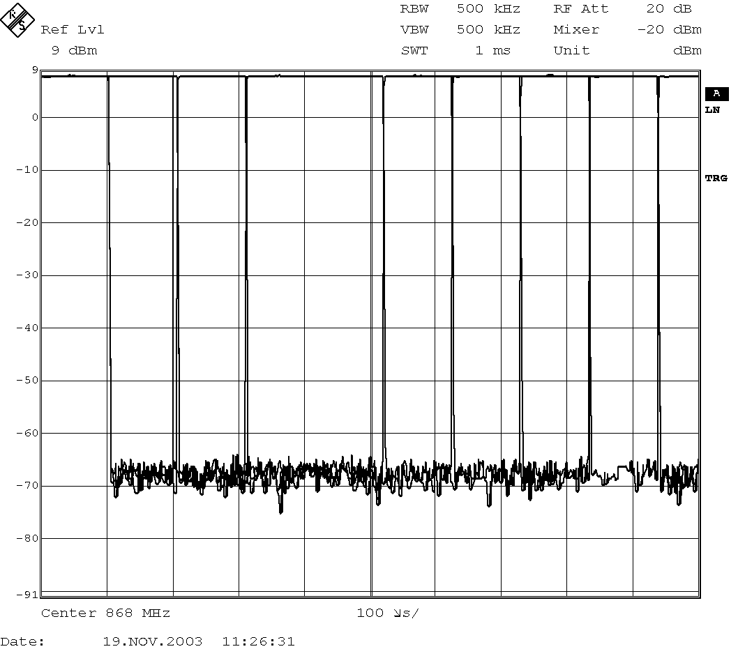
The data modulator can also provide OOK (On-Off Keying) modulation. OOK is an ASK (Amplitude Shift Keying) modulation using 100% modulation depth. OOK modulation is enabled in RX and in TX by setting TXDEV_M[3:0] = 0000 in the DEVIATION register. An OOK eye diagram is shown in Figure 5-29.
The data demodulator can also perform OOK demodulation. The demodulation is done by comparing the signal level with the “carrier sense” level (programmed as CS_LEVEL in the VGA4 register). The signal is then decimated and filtered in the data filter. Data decision and bit synchronization are as for FSK reception.
In this mode, AGC_AVG in the VGA2 register must be set to 3. The channel bandwidth must be 4 times the Baud rate for data rates up to 9.6 kBaud. For the highest data rates the channel bandwidth must be 2 times the Baud rate (see Table 5-14). Manchester coding must always be used for OOK.
NOTE
The automatic frequency control (AFC) cannot be used when receiving OOK, as it requires a frequency shift.
The AGC has a certain time-constant determined by FILTER_CLK, which depends on the IF filter bandwidth. There is a lower limit on FILTER_CLK and hence the AGC time constant. For very low data rates the minimum time constant is too fast and the AGC will increase the gain when a “0” is received and decrease the gain when a “1” is received. For this reason the minimum data rate in OOK is 2.4 kBaud.
Typical figures for the receiver sensitivity (BER = 10–3) are shown in Table 5-14 for OOK.

| 9.6 kBaud |
Table 5-14 Typical Receiver Sensitivity as a Function of Data Rate at 433 and 868 MHz, OOK Modulation, BER = 10–3, Pseudo-random Data (PN9 Sequence)
| DATA RATE
[kBaud] |
FILTER BW
[kHz] |
SENSITIVITY [dBm] | |
|---|---|---|---|
| 433 MHz
MANCHESTER MODE |
868 MHz
MANCHESTER MODE |
||
| 2.4 | 9.6 | –116 | — |
| 4.8 | 19.2 | –113 | –107 |
| 9.6 | 38.4 | –103 | –104 |
| 19.2 | 51.2 | –102 | –101 |
| 38.4 | 102.4 | –95 | –97 |
| 76.8 | 153.6 | –92 | –94 |
| 153.6 | 307.2 | –81 | –87 |