JAJSMK4B February   2017  – July 2024 CC3120

PRODUCTION DATA  

  1.   1
  2. 特長
  3. アプリケーション
  4. 概要
  5. 機能ブロック図
  6. Device Comparison
    1. 5.1 Related Products
  7. Terminal Configuration and Functions
    1. 6.1 Pin Diagram
    2. 6.2 Pin Attributes
    3. 6.3 Connections for Unused Pins
  8. Specifications
    1. 7.1  Absolute Maximum Ratings
    2. 7.2  ESD Ratings
    3. 7.3  Power-On Hours (POH)
    4. 7.4  Recommended Operating Conditions
    5. 7.5  Current Consumption Summary
    6. 7.6  TX Power and IBAT versus TX Power Level Settings
    7. 7.7  Brownout and Blackout Conditions
    8. 7.8  Electrical Characteristics (3.3 V, 25°C)
    9. 7.9  WLAN Receiver Characteristics
    10. 7.10 WLAN Transmitter Characteristics
    11. 7.11 WLAN Filter Requirements
      1. 7.11.1 WLAN Filter Requirements
    12. 7.12 Thermal Resistance Characteristics
      1. 7.12.1 Thermal Resistance Characteristics for RGK Package
    13. 7.13 Reset Requirement
    14. 7.14 Timing and Switching Characteristics
      1. 7.14.1 Power Supply Sequencing
      2. 7.14.2 Device Reset
      3. 7.14.3 Reset Timing
        1. 7.14.3.1 nRESET (32-kHz Crystal)
        2. 7.14.3.2 First-Time Power-Up and Reset Removal Timing Requirements (32-kHz Crystal)
        3. 7.14.3.3 nRESET (External 32-kHz)
          1. 7.14.3.3.1 First-Time Power-Up and Reset Removal Timing Requirements (External 32-kHz)
      4. 7.14.4 Wakeup From HIBERNATE Mode
        1. 7.14.4.1 nHIB Timing Requirements
      5. 7.14.5 Clock Specifications
        1. 7.14.5.1 Slow Clock Using Internal Oscillator
          1. 7.14.5.1.1 RTC Crystal Requirements
        2. 7.14.5.2 Slow Clock Using an External Clock
          1. 7.14.5.2.1 External RTC Digital Clock Requirements
        3. 7.14.5.3 Fast Clock (Fref) Using an External Crystal
          1. 7.14.5.3.1 WLAN Fast-Clock Crystal Requirements
        4. 7.14.5.4 Fast Clock (Fref) Using an External Oscillator
          1. 7.14.5.4.1 External Fref Clock Requirements (–40°C to +85°C)
      6. 7.14.6 Interfaces
        1. 7.14.6.1 Host SPI Interface Timing
          1. 7.14.6.1.1 Host SPI Interface Timing Parameters
        2. 7.14.6.2 Flash SPI Interface Timing
          1. 7.14.6.2.1 Flash SPI Interface Timing Parameters
    15. 7.15 External Interfaces
      1. 7.15.1 SPI Flash Interface
        1. 7.15.1.1 SPI Flash Interface
      2. 7.15.2 SPI Host Interface
        1. 7.15.2.1 SPI Host Interface
      3. 7.15.3 Host UART Interface
        1. 7.15.3.1 SimpleLink™ UART Configuration
        2. 7.15.3.2 5-Wire UART Topology
        3. 7.15.3.3 4-Wire UART Topology
        4. 7.15.3.4 3-Wire UART Topology
  9. Detailed Description
    1. 8.1 Device Features
      1. 8.1.1 WLAN
      2. 8.1.2 Network Stack
      3. 8.1.3 Security
      4. 8.1.4 Host Interface and Driver
      5. 8.1.5 System
    2. 8.2 Power-Management Subsystem
      1. 8.2.1 VBAT Wide-Voltage Connection
      2. 8.2.2 Preregulated 1.85V
    3. 8.3 Low-Power Operating Modes
      1. 8.3.1 Low-Power Deep Sleep
      2. 8.3.2 Hibernate
      3. 8.3.3 Shutdown
    4. 8.4 Memory
      1. 8.4.1 External Memory Requirements
    5. 8.5 Restoring Factory Default Configuration
  10. Applications, Implementation, and Layout
    1. 9.1 Application Information
      1. 9.1.1 Typical Application—CC3120R Wide-Voltage Mode
      2. 9.1.2 Typical Application Schematic—CC3120R Preregulated, 1.85-V Mode
    2. 9.2 PCB Layout Guidelines
      1. 9.2.1 General PCB Guidelines
      2. 9.2.2 Power Layout and Routing
        1. 9.2.2.1 Design Considerations
      3. 9.2.3 Clock Interfaces
      4. 9.2.4 Digital Input and Output
      5. 9.2.5 RF Interface
  11. 10Device and Documentation Support
    1. 10.1 Development Tools and Software
    2. 10.2 Firmware Updates
    3. 10.3 Device Nomenclature
    4. 10.4 Documentation Support
    5. 10.5 サポート・リソース
    6. 10.6 Trademarks
    7. 10.7 静電気放電に関する注意事項
    8. 10.8 Export Control Notice
    9. 10.9 用語集
  12. 11Revision History
  13. 12Mechanical, Packaging, and Orderable Information
    1. 12.1 Packaging Information

パッケージ・オプション

メカニカル・データ(パッケージ|ピン)
サーマルパッド・メカニカル・データ
発注情報

Fast Clock (Fref) Using an External Oscillator

The CC3120R device can accept an external TCXO/XO for the 40-MHz clock. In this mode of operation, the clock is connected to WLAN_XTAL_P (pin 23). WLAN_XTAL_N (pin 22) is connected to GND. The external TCXO/XO can be enabled by TCXO_EN (pin 21) from the device to optimize the power consumption of the system.

If the TCXO does not have an enable input, an external LDO with an enable function can be used. Using the LDO improves noise on the TCXO power supply.

Figure 7-12 shows the connection.
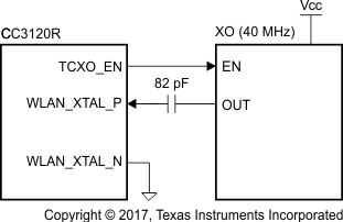
CC3120 External TCXO Input Figure 7-12 External TCXO Input


Section 7.14.5.4.1 lists the external Fref clock requirements.