JAJSIK6C February 2020 – December 2024 CC3235MODAS , CC3235MODASF , CC3235MODS , CC3235MODSF
PRODUCTION DATA
- 1
- 1 特長
- 2 アプリケーション
- 3 概要
- 4 機能ブロック図
- 5 Device Comparison
- 6 Pin Configuration and Functions
-
7 Specifications
- 7.1 Absolute Maximum Ratings
- 7.2 ESD Ratings
- 7.3 Recommended Operating Conditions
- 7.4 Current Consumption (CC3235MODS and CC3235MODAS)
- 7.5 Current Consumption (CC3235MODSF and CC3235MODASF)
- 7.6 TX Power Control for 2.4 GHz Band
- 7.7 TX Power Control for 5 GHz
- 7.8 Brownout and Blackout Conditions
- 7.9 Electrical Characteristics for GPIO Pins
- 7.10 CC3235MODAx Antenna Characteristics
- 7.11 WLAN Receiver Characteristics
- 7.12 WLAN Transmitter Characteristics
- 7.13 BLE and WLAN Coexistence Requirements
- 7.14 Reset Requirement
- 7.15 Thermal Resistance Characteristics for MOB and MON Packages
- 7.16
Timing and Switching Characteristics
- 7.16.1 Power-Up Sequencing
- 7.16.2 Power-Down Sequencing
- 7.16.3 Device Reset
- 7.16.4 Wake Up From Hibernate Timing
- 7.16.5 Peripherals Timing
-
8 Detailed Description
- 8.1 Overview
- 8.2 Functional Block Diagram
- 8.3 Arm Cortex-M4 Processor Core Subsystem
- 8.4 Wi-Fi Network Processor Subsystem
- 8.5 Security
- 8.6 FIPS 140-2 Level 1 Certification
- 8.7 Power-Management Subsystem
- 8.8 Low-Power Operating Mode
- 8.9 Memory
- 8.10 Restoring Factory Default Configuration
- 8.11 Boot Modes
- 8.12 Hostless Mode
- 8.13 Device Certification and Qualification
- 8.14 Module Markings
- 8.15 End Product Labeling
- 8.16 Manual Information to the End User
- 9 Applications, Implementation, and Layout
- 10Environmental Requirements and SMT Specifications
- 11Device and Documentation Support
- 12Revision History
- 13Mechanical, Packaging, and Orderable Information
パッケージ・オプション
デバイスごとのパッケージ図は、PDF版データシートをご参照ください。
メカニカル・データ(パッケージ|ピン)
- MOB|63
サーマルパッド・メカニカル・データ
発注情報
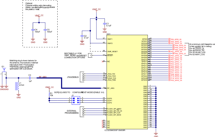
9.1.3 Typical Application Schematic (CC3235MODx)
Figure 9-3 shows the typical application schematic using the CC3235MODx module. See the full reference schematic for CC3235MODx.
Note that the CC3235MODx and CC3235MODAx modules share the same reference schematic. The difference between the two references is the antenna and its matching circuitry. The CC3235MODAx's pin 31 is not accessible to the designer because it is directly tied to the integrated antenna.
The following guidelines are recommended for implementation of the RF design:
- Ensure an RF path is designed with an impedance of 50Ω.
- Tuning of the antenna impedance π matching network is recommended after manufacturing of the PCB to account for PCB parasitics.
- π or L matching and tuning may be required between cascaded passive components on the RF path.
 Figure 9-3 CC3235MODx Typical Application Schematic
Table 9-1 provides the bill of materials for a typical application using the CC3235MODx module in Figure 9-3.
For full operation reference design, see the CC3235MODAx SimpleLink™ and Internet of Things Hardware Design Files.
| QTY | PART REFERENCE | VALUE | MANUFACTURER | PART NUMBER | DESCRIPTION |
|---|---|---|---|---|---|
| 2 | C1, C2 | 0.1µF | Murata | GRM155R61A104KA01D | Capacitor, ceramic, 0.1µF, 10V, ±10%, X5R, 0402 |
| 1 | C3 | 1pF | Murata | GRM1555C1H1R0CA01D | Capacitor, ceramic, 1pF, 50V, ±5%, C0G/NP0, 0402 |
| 2 | C4, C5 | 100µF | Murata | LMK325ABJ107MMHT | Capacitor, ceramic, 100µF, 10V, ±20%, X5R, AEC-Q200 Grade 3, 1210 |
| 1 | E1 | 2.4GHz, 5GHz Ant | Ethertronics | M830520 | Antenna Bluetooth WLAN Zigbee® |
| 1 | L1 | 4.7nH | Murata | LQG15HS4N7C02D | Inductor, Multilayer, Air Core, 4.7nH, 0.7 A, 0.16Ω, SMD |
| 1 | R1 | 10k | Vishay-Dale | CRCW040210K0JNED | RES, 10k, 5%, 0.063 W, AEC-Q200 Grade 0, 0402 |
| 1 | CC1 | CC3235MODx | Texas Instruments | CC3235MODSM2MOB/CC3235MODSF12MOB | SimpleLink™ Wi-Fi® and Internet-of-Things Module Solution, a Single-Chip Wireless Dual-Band MCU, MOB0063A |