JAJSIK6C February   2020  – December 2024 CC3235MODAS , CC3235MODASF , CC3235MODS , CC3235MODSF

PRODUCTION DATA  

  1.   1
  2. 特長
  3. アプリケーション
  4. 概要
  5. 機能ブロック図
  6. Device Comparison
    1. 5.1 Related Products
  7. Pin Configuration and Functions
    1. 6.1 CC3235MODx and CC3235MODAx Pin Diagram
    2. 6.2 Pin Attributes and Pin Multiplexing
      1. 6.2.1 Module Pin Descriptions
    3. 6.3 Signal Descriptions
    4. 6.4 Drive Strength and Reset States for Analog-Digital Multiplexed Pins
    5. 6.5 Pad State After Application of Power to Chip, but Before Reset Release
    6. 6.6 Connections for Unused Pins
  8. Specifications
    1. 7.1  Absolute Maximum Ratings
    2. 7.2  ESD Ratings
    3. 7.3  Recommended Operating Conditions
    4. 7.4  Current Consumption (CC3235MODS and CC3235MODAS)
      1.      21
      2.      22
    5. 7.5  Current Consumption (CC3235MODSF and CC3235MODASF)
      1.      24
      2.      25
    6. 7.6  TX Power Control for 2.4 GHz Band
    7. 7.7  TX Power Control for 5 GHz
    8. 7.8  Brownout and Blackout Conditions
    9. 7.9  Electrical Characteristics for GPIO Pins
      1. 7.9.1 Electrical Characteristics for Pin Internal Pullup and Pulldown (25°C)
    10. 7.10 CC3235MODAx Antenna Characteristics
    11. 7.11 WLAN Receiver Characteristics
      1.      33
      2.      34
    12. 7.12 WLAN Transmitter Characteristics
      1.      36
      2.      37
    13. 7.13 BLE and WLAN Coexistence Requirements
    14. 7.14 Reset Requirement
    15. 7.15 Thermal Resistance Characteristics for MOB and MON Packages
    16. 7.16 Timing and Switching Characteristics
      1. 7.16.1 Power-Up Sequencing
      2. 7.16.2 Power-Down Sequencing
      3. 7.16.3 Device Reset
      4. 7.16.4 Wake Up From Hibernate Timing
      5. 7.16.5 Peripherals Timing
        1. 7.16.5.1  SPI
          1. 7.16.5.1.1 SPI Master
          2. 7.16.5.1.2 SPI Slave
        2. 7.16.5.2  I2S
          1. 7.16.5.2.1 I2S Transmit Mode
          2. 7.16.5.2.2 I2S Receive Mode
        3. 7.16.5.3  GPIOs
          1. 7.16.5.3.1 GPIO Input Transition Time Parameters
        4. 7.16.5.4  I2C
        5. 7.16.5.5  IEEE 1149.1 JTAG
        6. 7.16.5.6  ADC
        7. 7.16.5.7  Camera Parallel Port
        8. 7.16.5.8  UART
        9. 7.16.5.9  External Flash Interface
        10. 7.16.5.10 SD Host
        11. 7.16.5.11 Timers
  9. Detailed Description
    1. 8.1  Overview
    2. 8.2  Functional Block Diagram
    3. 8.3  Arm Cortex-M4 Processor Core Subsystem
    4. 8.4  Wi-Fi Network Processor Subsystem
      1. 8.4.1 WLAN
      2. 8.4.2 Network Stack
    5. 8.5  Security
    6. 8.6  FIPS 140-2 Level 1 Certification
    7. 8.7  Power-Management Subsystem
      1. 8.7.1 VBAT Wide-Voltage Connection
    8. 8.8  Low-Power Operating Mode
    9. 8.9  Memory
      1. 8.9.1 Internal Memory
        1. 8.9.1.1 SRAM
        2. 8.9.1.2 ROM
        3. 8.9.1.3 Flash Memory
        4. 8.9.1.4 Memory Map
    10. 8.10 Restoring Factory Default Configuration
    11. 8.11 Boot Modes
      1. 8.11.1 Boot Mode List
    12. 8.12 Hostless Mode
    13. 8.13 Device Certification and Qualification
      1. 8.13.1 FCC Certification and Statement
      2. 8.13.2 IC/ISED Certification and Statement
      3. 8.13.3 ETSI/CE Certification
      4. 8.13.4 MIC Certification
    14. 8.14 Module Markings
    15. 8.15 End Product Labeling
    16. 8.16 Manual Information to the End User
  10. Applications, Implementation, and Layout
    1. 9.1 Typical Application
      1. 9.1.1 BLE/2.4GHz Radio Coexistence
      2. 9.1.2 Antenna Selection (CC3235MODx only)
      3. 9.1.3 Typical Application Schematic (CC3235MODx)
      4. 9.1.4 Typical Application Schematic (CC3235MODAx)
    2. 9.2 Device Connection and Layout Fundamentals
      1. 9.2.1 Power Supply Decoupling and Bulk Capacitors
      2. 9.2.2 Reset
      3. 9.2.3 Unused Pins
    3. 9.3 PCB Layout Guidelines
      1. 9.3.1 General Layout Recommendations
      2. 9.3.2 CC3235MODx RF Layout Recommendations
        1. 9.3.2.1 Antenna Placement and Routing
        2. 9.3.2.2 Transmission Line Considerations
      3. 9.3.3 CC3235MODAx RF Layout Recommendations
  11. 10Environmental Requirements and SMT Specifications
    1. 10.1 PCB Bending
    2. 10.2 Handling Environment
      1. 10.2.1 Terminals
      2. 10.2.2 Falling
    3. 10.3 Storage Condition
      1. 10.3.1 Moisture Barrier Bag Before Opened
      2. 10.3.2 Moisture Barrier Bag Open
    4. 10.4 PCB Assembly Guide
      1. 10.4.1 PCB Land Pattern and Thermal Vias
      2. 10.4.2 SMT Assembly Recommendations
      3. 10.4.3 PCB Surface Finish Requirements
      4. 10.4.4 Solder Stencil
      5. 10.4.5 Package Placement
      6. 10.4.6 Solder Joint Inspection
      7. 10.4.7 Rework and Replacement
      8. 10.4.8 Solder Joint Voiding
    5. 10.5 Baking Conditions
    6. 10.6 Soldering and Reflow Condition
  12. 11Device and Documentation Support
    1. 11.1 Development Tools and Software
    2. 11.2 Firmware Updates
    3. 11.3 Device Nomenclature
    4. 11.4 Documentation Support
    5. 11.5 Related Links
    6. 11.6 サポート・リソース
    7. 11.7 Trademarks
    8. 11.8 静電気放電に関する注意事項
    9. 11.9 用語集
  13. 12Revision History
  14. 13Mechanical, Packaging, and Orderable Information
    1. 13.1 Mechanical, Land, and Solder Paste Drawings
    2. 13.2 Package Option Addendum
      1. 13.2.1 Packaging Information
      2. 13.2.2 Tape and Reel Information
      3. 13.2.3 CC3235MODx Tape Specifications
      4. 13.2.4 CC3235MODAx Tape Specifications

パッケージ・オプション

デバイスごとのパッケージ図は、PDF版データシートをご参照ください。

メカニカル・データ(パッケージ|ピン)
  • MOB|63
サーマルパッド・メカニカル・データ
発注情報

BLE/2.4GHz Radio Coexistence

The CC3235MODx and CC3235MODAx devices are designed to support BLE/2.4GHz radio coexistence. Because WLAN is inherently more tolerant to time-domain disturbances, the coexistence mechanism gives priority to the Bluetooth® low energy entity over the WLAN. Bluetooth® low energy operates in the 2.4GHz band, therefore the coexistence mechanism does not affect the 5GHz band. The CC3235MODx andCC3235MODAx device can operate normally on the 5GHz band, while the Bluetooth® low energy works on the 2.4GHz band without mutual interference.

The following coexistence modes can be configured by the user:

  • Off mode or intrinsic mode

    • No BLE/2.4GHz radio coexistence, or no synchronization between WLAN and Bluetooth® low energy—in case Bluetooth® low energy exists in this mode, collisions can randomly occur.

  • Time Division Multiplexing (TDM, Dual Antenna)
    • Dual-band Wi-Fi (see Figure 9-1)

      In this mode, the WLAN can operate on either a 2.4 or 5GHz band and Bluetooth® low energy operates on the 2.4GHz band.

Figure 9-1 shows the dual antenna implementation of a complete Bluetooth® low energy and WLAN coexistence network with the WLAN operating on either a 2.4 or a 5GHz band. Note in this implementation a Coex switch is not required and only a single GPIO from the BLE device to the CC3235MOD device is needed. In addition, the CC3235MODx's antenna is external while the CC3235MODAx's antenna is integrated.
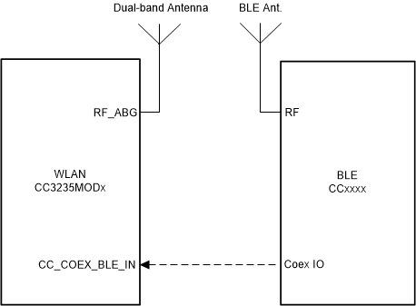
CC3235MODS CC3235MODSF CC3235MODAS CC3235MODASF Dual-Antenna Coexistence Mode Block DiagramFigure 9-1 Dual-Antenna Coexistence Mode Block Diagram