JAJSGW3E April 2019 – December 2024 CC3235S , CC3235SF
PRODUCTION DATA
- 1
- 1 特長
- 2 アプリケーション
- 3 概要
- 4 機能ブロック図
- 5 Device Comparison
- 6 Pin Configuration and Functions
-
7 Specifications
- 7.1 Absolute Maximum Ratings
- 7.2 ESD Ratings
- 7.3 Power-On Hours (POH)
- 7.4 Recommended Operating Conditions
- 7.5 Current Consumption Summary (CC3235S)
- 7.6 Current Consumption Summary (CC3235SF)
- 7.7 TX Power Control for 2.4 GHz Band
- 7.8 TX Power Control for 5 GHz
- 7.9 Brownout and Blackout Conditions
- 7.10 Electrical Characteristics for GPIO Pins
- 7.11 Electrical Characteristics for Pin Internal Pullup and Pulldown
- 7.12 WLAN Receiver Characteristics
- 7.13 WLAN Transmitter Characteristics
- 7.14 WLAN Transmitter Out-of-Band Emissions
- 7.15 BLE/2.4 GHz Radio Coexistence and WLAN Coexistence Requirements
- 7.16 Thermal Resistance Characteristics for RGK Package
- 7.17
Timing and Switching Characteristics
- 7.17.1 Power Supply Sequencing
- 7.17.2 Device Reset
- 7.17.3 Reset Timing
- 7.17.4 Wakeup From HIBERNATE Mode
- 7.17.5 Clock Specifications
- 7.17.6 Peripherals Timing
- 8 Detailed Description
- 9 Applications, Implementation, and Layout
- 10Device and Documentation Support
- 11Revision History
- 12Mechanical, Packaging, and Orderable Information
9.1.3 Typical Application
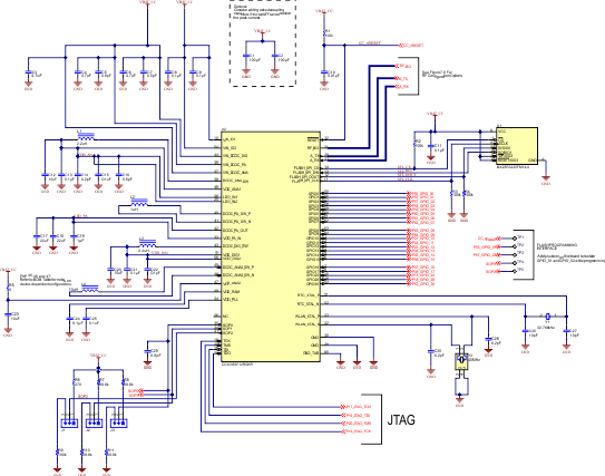
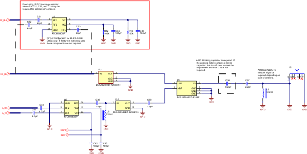
Figure 9-7 shows the schematic of the engine area for the CC3235x device in the wide-voltage mode of operation, with the corresponding bill of materials show in Table 9-1. Figure 9-8 provides the schematic for the RF implementation with and without BLE/2.4GHz coexistence, with the corresponding bill of materials shown in Table 9-2. For a full operation reference design, see the CC3235x SimpleLink™ and Internet of Things Hardware Design Files.
 Figure 9-7 CC3235x Engine Area
Table 9-1 Bill of Materials for CC3235x Engine Area
| Quantity | Designator | Value | Manufacturer | Part Number | Description |
|---|---|---|---|---|---|
| 2 | C1, C2 | 100 µF | Taiyo Yuden | LMK325ABJ107MMHT | CAP, CERM, 100 µF, 10 V, +/- 20%, X5R, AEC-Q200 Grade 3, 1210 |
| 3 | C3, C4, C6 | 4.7 µF | Taiyo Yuden | JMK105BC6475MV-F | CAP, CERM, 4.7 uF, 6.3 V, +/- 20%, X6S, 0402 |
| 3 | C5, C16, C29 | 0.6 pF | MuRata | GJM0335C1ER60BB01D | CAP, CERM, 0.6pF, 25 V, +/- 16%, C0G/NP0, 0201 |
| 1 | C7 | 0.5 pF | Murata | GJM0335C1ER50BB01D | CAP, CERM, 0.5 pF, 25 V, +/- 20%, C0G/NP0, 0201 |
| 7 | C8, C9, C11, C13, C21, C22, C24 | 0.1 µF | Walsin | CL05B104KO5NNNC | CAP, CERM, 0.1 µF, 16 V, +/- 10%, X7R, 0402 |
| 1 | C10 | 0.01 µF | Walsin | 0402B103K500CT | CAP, CERM, 0.01 µF, 50 V, +/- 10%, X7R, 0402 |
| 3 | C12, C20, C23 | 10 µF | Taiyo Yuden | LMK107BC6106MA-T | CAP, CERM, 10 uF, 10 V, +/- 20%, X6S, 0603 |
| 1 | C14 | 0.2 pF | MuRata | GJM0335C1ER20BB01D | CAP, CERM, 0.2pF, 25 V, +/- 50%, C0G/NP0, 0201 |
| 2 | C15, C25 | 0.1 µF | Samsung Electro-Mechanics | CL03A104KP3NNNC | CAP, CERM, 0.1 uF, 10 V, +/- 10%, X5R, 0201 |
| 2 | C17, C18 | 22 µF | MuRata | GRM188C80G226ME15J | CAP, CERM, 22 uF, 4 V, +/- 20%, X6S, 0603 |
| 1 | C19 | 1 µF | Walsin | CL05A105MP5NNNC | CAP, CERM, 1 µF, 10 V, +/- 20%, X5R, 0402 |
| 2 | C26, C27 | 10 pF | Walsin | 0402N100J500CT | CAP, CERM, 10 pF, 50 V, +/- 5%, C0G/NP0, 0402 |
| 2 | C28, C30 | 6.2 pF | Walsin | 0402N6R2C500CT | CAP, CERM, 6.2 pF, 50 V, +/- 4%, C0G/NP0, 0402 |
| 3 | J1, J2, J3 | Wurth Elektronik | 61300311121 | Header, 2.54 mm, 3x1, Gold, TH | |
| 2 | L1, L3 | 2.2 µH | MuRata | LQM2MPN2R2NG0 | Inductor, Multilayer, Ferrite, 2.2 uH, 1.2 A, 0.11 ohm, SMD |
| 1 | L2 | 1 µH | MuRata | LQM2HPN1R0MG0L | Inductor, Multilayer, Ferrite, 1 uH, 1.6 A, 0.055 ohm, SMD |
| 1 | L4(1) | 10 µH | TDK | MLP2520S100MT0S1 | Inductor, Multilayer, Ferrite, 10 uH, 0.7 A, 0.364 ohm, SMD |
| 5 | R1, R2, R3, R4, R9 | 100k | Vishay-Dale | CRCW0402100KJNED | RES, 100 k, 5%, 0.063 W, AEC-Q200 Grade 0, 0402 |
| 1 | R5(2) | 0 | Panasonic | ERJ-2GE0R00X | RES, 0, 5%, 0.063 W, 0402 |
| 1 | R6 | 270 | Vishay-Dale | CRCW0402270RJNED | RES, 270, 5%, 0.063 W, AEC-Q200 Grade 0, 0402 |
| 4 | R7, R8, R10, R11 | 69.8k | Vishay-Dale | CRCW040269K8FKED | RES, 69.8 k, 1%, 0.063 W, AEC-Q200 Grade 0, 0402 |
| 1 | U1 | Macronix International Co., LTD | MX25R3235FM1IL0 | Ultra low power, 32M-bit [x 1/x 2/x 4] CMOS MXSMIO(serial multi I/O) Flash memory, SOP-8 | |
| 1 | U2 | Texas Instruments | CC3235SF12RGKR | SimpleLink Wi-Fi and Internet-of-Things Solution, a Single-Chip Wireless MCU, RGK0064B (VQFN-64) | |
| 1 | Y1 | Abracon Corporation | ABS07-32.768KHZ-9-T | Crystal, 32.768KHz, 9PF, SMD | |
| 1 | Y2 | TXC Corporation | 8Y40072002 | Crystal, 40 MHz, 8 pF, SMD |
(1) For the CC3235SF device, L4 is populated. For the CC3235S device, L4 is not populated.
(2) For the CC3220SF device, R5 is not populated. For the CC3235S device if R5 is populated, Pin 45 can be used as GPIO_31.
 Figure 9-8 CC3235x RF Schematic Implementation with and without Coexistence
Note:
The Following guidelines are recommended for implementation of the RF design:
- Ensure an RF path is designed with an impedance of 50Ω.
- Tuning of the antenna impedance π matching network is recommended after manufacturing of the PCB to account for PCB parasitics.
- π or L matching and tuning may be required between cascaded passive components on the RF path.
Table 9-2 Bill of Materials For CC3235x RF Section
| Quantity | Designator | Value | Manufacturer | Part Number | Description |
|---|---|---|---|---|---|
| 3 | C31(1), C32(1), C33(1) | 68 pF | Murata | GRM0335C1H680JA1D | CAP, CERM, 68 pF, 50 V, +/- 5%, C0G/NP0, 0201 |
| 4 | C34(1), C35(1), C42, C43 | 100 pF | Yageo | CC0201JRNPO8BN101 | CAP, CERM, 100 pF, 25 V, +/- 5%, C0G/NP0, 0201 |
| 1 | C36 | 8.2 pF | Walsin | 0402N8R2C500CT | CAP, CERM, 8.2 pF, 50 V, +/- 3%, C0G/NP0, 0402 |
| 1 | C37 | 2.2 pF | MuRata | GJM1555C1H2R2BB01D | CAP, CERM, 2.2 pF, 50 V, +/- 4.5%, C0G/NP0, 0402 |
| 1 | C38 | 1.6 pF | MuRata | GRM0335C1H1R6BA01D | CAP, CERM, 1.6 pF, 50 V, +/- 7%, C0G/NP0, 0201 |
| 1 | C39 | 1.9 pF | MuRata | GJM1555C1H1R9WB01D | CAP, CERM, 1.9 pF, 50 V, +/- 2.6%, C0G/NP0, 0402 |
| 2 | C40, C41 | 4.7 pF | MuRata | GRM0335C1H4R7BA01D | CAP, CERM, 4.7 pF, 50 V, +/- 3%, C0G/NP0, 0201 |
| 1 | E1 | Ethertronics | M830520 | WLAN Antenna 802.11, SMD | |
| 1 | FL1 | TDK | DEA202450BT-1294C1-H | Multilayer Chip Band Pass Filter For 2.4 GHz W-LAN/Bluetooth, SMD | |
| 1 | FL2 | TDK | DEA165538BT-2236B1-H | Multilayer Band Pass Filter For 5 GHz W-LAN/LTE-U | |
| 1 | L5 | 3.9 nH | MuRata | LQG15HS3N9S02D | Inductor, Multilayer, Air Core, 3.9 nH, 0.75 A, 0.14 ohm, SMD |
| 1 | L6 | 2.7 nH | MuRata | LQG15WH2N7C02D | Inductor, Multilayer, Air Core, 2.7 nH, 0.9 A, 0.07 ohm, AEC-Q200 Grade 1, SMD |
| 2 | R12(1), R13(1) | 100k | Vishay-Dale | CRCW0402100KJNED | RES, 100 k, 5%, 0.063 W, AEC-Q200 Grade 0, 0402 |
| 2 | U3(1), U5 | Richwave | RTC6608OSP | 0.03 GHz-6 GHz SPDT Switch | |
| 1 | U4 | TDK | DPX165950DT-8148A1 | Multilayer Diplexer for 2.4 GHz W-LAN & Bluetooth / 5 GHz W-LAN |
(1) If the BLE/2.4GHz coexistence features is not used, these components are not required.