JAJSH80C august 1998 – march 2023 CD4051B-Q1 , CD4053B-Q1
PRODUCTION DATA
- 1 特長
- 2 アプリケーション
- 3 概要
- 4 Revision History
- 5 Pin Configuration and Functions
-
6 Specifications
- 6.1 Absolute Maximum Ratings
- 6.2 ESD Ratings
- 6.3 Recommended Operating Conditions
- 6.4 Thermal Information
- 6.5 Electrical Characteristics - CD4051B-Q1
- 6.6 AC Performance Characteristics - CD4051B-Q1
- 6.7 Electrical Characteristics - CD4053B-Q1
- 6.8 AC Performance Characteristics - CD4053B-Q1
- 6.9 Typical Characteristics
- 7 Parameter Measurement Information
- 8 Detailed Description
- 9 Application and Implementation
- 10Device and Documentation Support
- 11Mechanical, Packaging, and Orderable Information
7 Parameter Measurement Information
 Figure 7-1 Typical
Bias Voltages
Figure 7-1 Typical
Bias VoltagesNote:
The ADDRESS (digital-control
inputs) and INHIBIT logic levels are: 0 = VSS
and 1 = VDD. The analog signal
(through the TG) may swing from VEE to VDD.
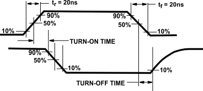 Figure 7-2 Waveforms, Channel Being Turned ON (RL = 1 kΩ)
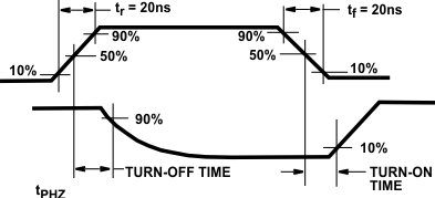 Figure 7-3 Waveforms, Channel Being Turned OFF (RL = 1 kΩ)
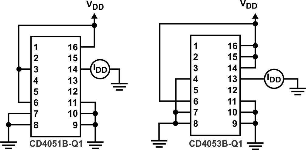 Figure 7-4 OFF
Channel Leakage Current – Any Channel OFF
 Figure 7-5 On Channel Leakage Current –
Any Channel On
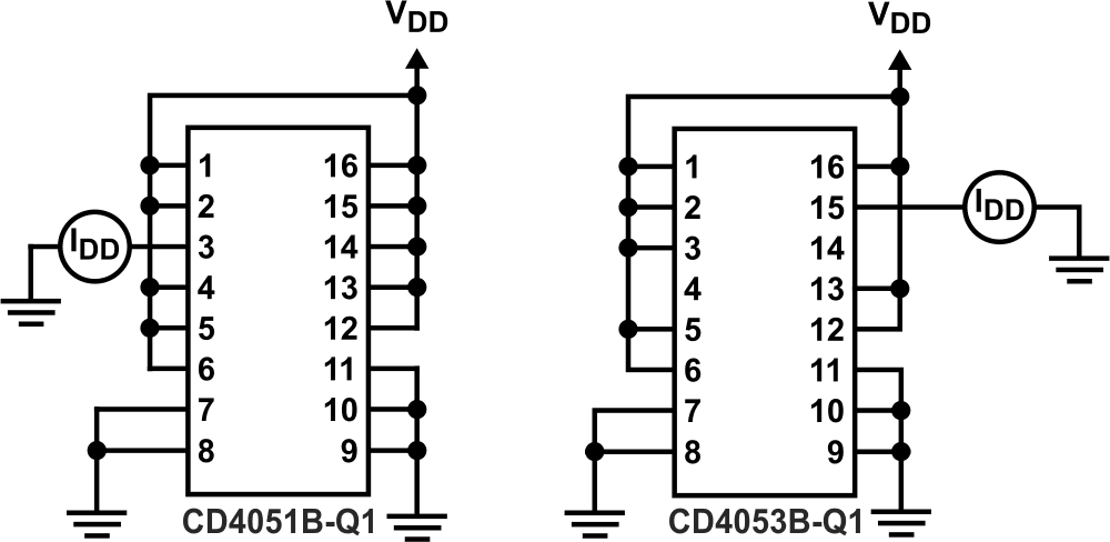 Figure 7-6 OFF
Channel Leakage Current – All Channels OFF
 Figure 7-7 Propagation Delay – Address Input to Signal Output
 Figure 7-8 Propagation Delay – Inhibit Input to Signal Output
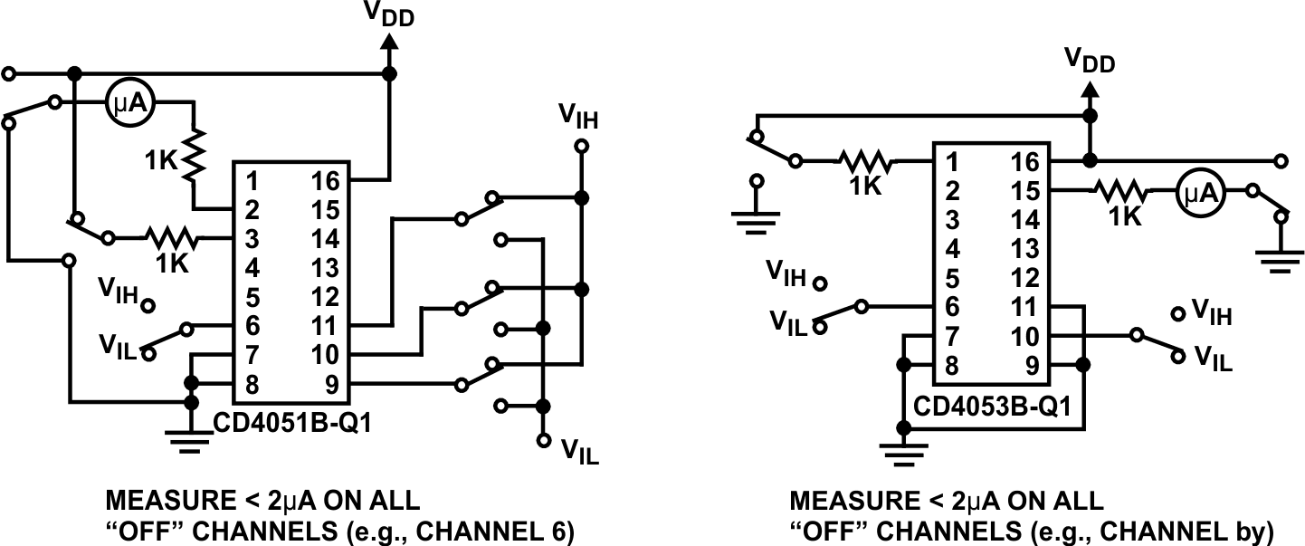 Figure 7-9 Input
Voltage Test Circuits (Noise Immunity)
 Figure 7-10 Quiescent Device Current
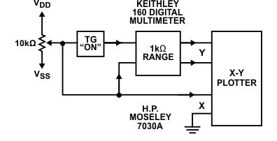 Figure 7-11 Channel ON Resistance Measurement Circuit
 Figure 7-12 Input
Current
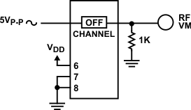 Figure 7-13 Feed-Through (All Types)
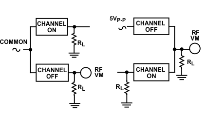 Figure 7-14 Crosstalk Between Any Two Channels (All Types)
 Figure 7-15 Crosstalk
Between Duals or Triplets (CD4053B-Q1)
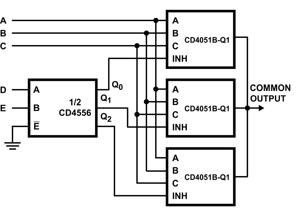 Figure 7-16 24-to-1
MUX Addressing