JAJSUX9D June 2003 – August 2024 CD4067B , CD4097B
PRODUCTION DATA
- 1
- 1 特長
- 2 アプリケーション
- 3 概要
- 4 Pin Configuration and Functions
- 5 Specifications
- 6 Parameter Measurement Information
- 7 Detailed Description
- 8 Application and Implementation
- 9 Device and Documentation Support
- 10Revision History
- 11Mechanical, Packaging, and Orderable Information
パッケージ・オプション
デバイスごとのパッケージ図は、PDF版データシートをご参照ください。
メカニカル・データ(パッケージ|ピン)
- DW|24
- PW|24
サーマルパッド・メカニカル・データ
発注情報
6.1 Test Circuits
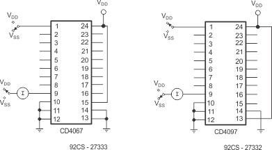 Figure 6-1 OFF Channel Leakage Current – Any Channel OFF
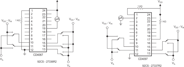 Figure 6-2 Input Voltage –Measure <2µA on all OFF Channels (For Example, Channel 12)
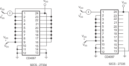 Figure 6-3 OFF Channel Leakage Current – All Channels OFF
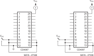 Figure 6-4 Quiescent Device Current
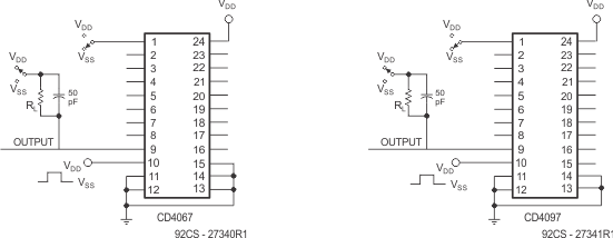 Figure 6-5 Turn-on and Turn-off Propagation Delay – Address Select Input to Signal Output (For Example,, Measured on Channel 0)
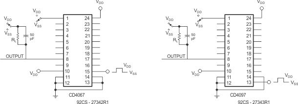 Figure 6-6 Turn-on and Turn-off Propagation Delay – Inhibit Input to Signal Output (For Example,, Measured on Channel 1)
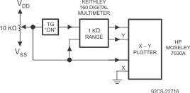 Figure 6-7 Channel ON Resistance Measurement Circuit
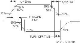 Figure 6-8 Propagation Delay Waveform Channel Being turned ON (RL = 10kΩ, CL = 50 pF)
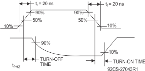 Figure 6-9 Propagation Delay Waveform Channel Being turned OFF (RL = 300Ω, CL = 50 pF)