JAJSOZ3B November 1998 – July 2022 CD54HC245 , CD54HCT245 , CD74HC245 , CD74HCT245
PRODUCTION DATA
- 1 特長
- 2 概要
- 3 Revision History
- 4 Pin Configuration and Functions
- 5 Specifications
- 6 Parameter Measurement Information
- 7 Detailed Description
- 8 Power Supply Recommendations
- 9 Layout
- 10Device and Documentation Support
- 11Mechanical, Packaging, and Orderable Information
パッケージ・オプション
デバイスごとのパッケージ図は、PDF版データシートをご参照ください。
メカニカル・データ(パッケージ|ピン)
- N|20
- DW|20
サーマルパッド・メカニカル・データ
発注情報
6 Parameter Measurement Information
tpd is the maximum between tPLH and tPHL
tt is the maximum between tTLH and tTHL
 Figure 6-1 HC transition times and
propagation delay times, combination logic
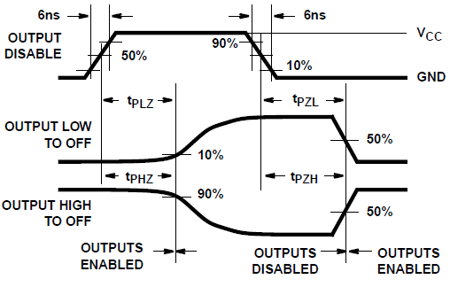
 Figure 6-3 HC three-state propagation
delay waveform
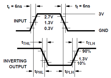
 Figure 6-2 HCT transition times and
propagation delay times, combination logic
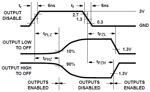
 Figure 6-4 HCT three-state
propagation delay waveform
 Figure 6-5 HC and HCT three-state
propagation delay test circuit