JAJSHG0N November 1997 – April 2024 CD54HC4051 , CD54HC4052 , CD54HC4053 , CD54HCT4051 , CD74HC4051 , CD74HC4052 , CD74HC4053 , CD74HCT4051 , CD74HCT4052 , CD74HCT4053
PRODUCTION DATA
- 1
- 1 特長
- 2 アプリケーション
- 3 概要
- 4 Pin Configuration and Functions
-
5 Specifications
- 5.1 Absolute Maximum Ratings
- 5.2 ESD Ratings
- 5.3 Thermal Information
- 5.4 Recommended Operating Conditions
- 5.5 Electrical Characteristics: HC Devices
- 5.6 Electrical Characteristics: HCT Devices
- 5.7 Switching Characteristics, VCC = 5V
- 5.8 Switching Characteristics, CL = 50pF
- 5.9 Analog Channel Specifications
- 5.10 Typical Characteristics
- 6 Parameter Measurement Information
- 7 Detailed Description
- 8 Application and Implementation
- 9 Device and Documentation Support
- 10Revision History
- 11Mechanical, Packaging, and Orderable Information
パッケージ・オプション
デバイスごとのパッケージ図は、PDF版データシートをご参照ください。
メカニカル・データ(パッケージ|ピン)
- N|16
- D|16
サーマルパッド・メカニカル・データ
発注情報
4 Pin Configuration and Functions
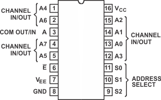
 Figure 4-1 CDx4HCx4051 J, N, D, NS, PW Packages 16-Pin
CDIP, PDIP, SOIC, SO, TSSOP (Top View)
 |
PIN |
TYPE(1) |
DESCRIPTION |
|
|---|---|---|---|
|
NAME |
NO. |
||
|
CH A4 IN/OUT |
1 |
I/O |
Channel 4 in/out |
|
CH A6 IN/OUT |
2 |
I/O | Channel 6 in/out |
|
COM OUT/IN |
3 |
I/O |
Common out/in |
|
CH A7 IN/OUT |
4 |
I/O | Channel 7 in/out |
|
CH A5 IN/OUT |
5 |
I/O | Channel 5 in/out |
|
!E |
6 |
I |
Enable Channels (Active Low) |
|
VEE |
7 |
— |
Negative power input |
|
GND |
8 |
— |
Ground |
|
S2 |
9 |
I |
Channel select 2 |
|
S1 |
10 |
I |
Channel select 1 |
|
S0 |
11 |
I |
Channel select 0 |
|
CH A3 IN/OUT |
12 |
I/O | Channel 3 in/out |
|
CH A0 IN/OUT |
13 |
I/O | Channel 0 in/out |
|
CH A1 IN/OUT |
14 |
I/O | Channel 1 in/out |
|
CH A2 IN/OUT |
15 |
I/O |
Channel 2 in/out |
|
VCC |
16 |
— |
Positive power input |
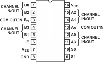
 Figure 4-2
CDx4HCx4052 J, N, D, NS, PW Packages 16-Pin CDIP, PDIP, SOIC, SO, TSSOP (Top
View)
 |
PIN |
TYPE(1) |
DESCRIPTION |
|
|---|---|---|---|
|
NAME |
NO. |
||
|
CH B0 IN/OUT |
1 |
I/O |
Channel B0 in/out |
|
CH B2 IN/OUT |
2 |
I/O |
Channel B2 in/out |
|
COM B OUT/IN |
3 |
I/O |
B common out/in |
|
CH B3 IN/OUT |
4 |
I/O |
Channel B3 in/out |
|
CH B1 IN/OUT |
5 |
I/O |
Channel B1 in/out |
|
!E |
6 |
I |
Enable channels (Active Low) |
|
VEE |
7 |
— |
Negative power input |
|
GND |
8 |
— |
Ground |
|
S1 |
9 |
I |
Channel select 1 |
|
S0 |
10 |
I |
Channel select 0 |
|
CH A3 IN/OUT |
11 |
I/O |
Channel A3 in/out |
|
CH A0 IN/OUT |
12 |
I/O |
Channel A0 in/out |
|
COM A IN/OUT |
13 |
I/O |
A common out/in |
|
CH A1 IN/OUT |
14 |
I/O |
Channel A1 in/out |
|
CH A2 IN/OUT |
15 |
I/O |
Channel A2 in/out |
|
VCC |
16 |
— |
Positive power input |
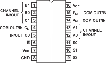
 Figure 4-3 CDx4HCx4053 J, N, D, NS, PW Packages 16-Pin CDIP, PDIP, SOIC, SO, TSSOP (Top
View)
 |
PIN |
TYPE(1) |
DESCRIPTION |
|
|---|---|---|---|
|
NAME |
NO. |
||
|
B1IN/OUT |
1 |
I/O |
B channel Y in/out |
|
B0 IN/OUT |
2 |
I/O |
B channel X in/out |
|
C1 IN/OUT |
3 |
I/O |
C channel Y in/out |
|
COM C OUT/IN |
4 |
I/O |
C common out/in |
|
C0 IN/OUT |
5 |
I/O |
C channel X in/out |
|
!E |
6 |
I |
Enable channels (Active Low) |
|
VEE |
7 |
— |
Negative power input |
|
GND |
8 |
— |
Ground |
|
S2 |
9 |
I |
Channel select 2 |
|
S1 |
10 |
I |
Channel select 1 |
|
S0 |
11 |
I |
Channel select 0 |
|
A0 IN/OUT |
12 |
I/O |
A channel X in/out |
|
A1 IN/OUT |
13 |
I/O |
A channel Y in/out |
|
COM A OUT/IN |
14 |
I/O |
A common out/in |
|
COM B OUT/IN |
15 |
I/O |
B common out/in |
|
VCC |
16 |
— |
Positive power input |