JAJSHG0N November 1997 – April 2024 CD54HC4051 , CD54HC4052 , CD54HC4053 , CD54HCT4051 , CD74HC4051 , CD74HC4052 , CD74HC4053 , CD74HCT4051 , CD74HCT4052 , CD74HCT4053
PRODUCTION DATA
- 1
- 1 特長
- 2 アプリケーション
- 3 概要
- 4 Pin Configuration and Functions
-
5 Specifications
- 5.1 Absolute Maximum Ratings
- 5.2 ESD Ratings
- 5.3 Thermal Information
- 5.4 Recommended Operating Conditions
- 5.5 Electrical Characteristics: HC Devices
- 5.6 Electrical Characteristics: HCT Devices
- 5.7 Switching Characteristics, VCC = 5V
- 5.8 Switching Characteristics, CL = 50pF
- 5.9 Analog Channel Specifications
- 5.10 Typical Characteristics
- 6 Parameter Measurement Information
- 7 Detailed Description
- 8 Application and Implementation
- 9 Device and Documentation Support
- 10Revision History
- 11Mechanical, Packaging, and Orderable Information
パッケージ・オプション
デバイスごとのパッケージ図は、PDF版データシートをご参照ください。
メカニカル・データ(パッケージ|ピン)
- PW|16
- N|16
- D|16
サーマルパッド・メカニカル・データ
発注情報
6 Parameter Measurement Information
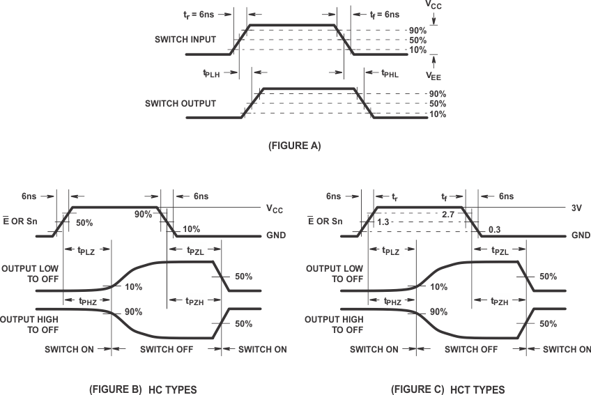 Figure 6-1 Switch Propagation Delay, Turn-On, Turn-Off
Times
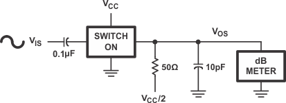 Figure 6-2 Frequency Response Test Circuit
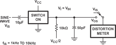 Figure 6-4 ¼Sine-Wave Distortion Test Circuit
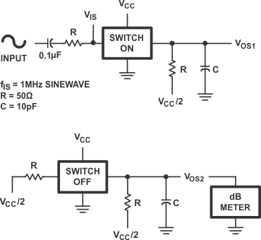 Figure 6-3 Crosstalk Between Two Switches Test Circuit
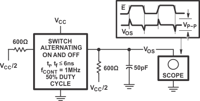 Figure 6-5 Control to Switch Feedthrough Noise Test Circuit
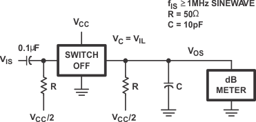 Figure 6-6 Switch
OFF Signal Feedthrough
 Figure 6-7 Switch
ON/OFF Propagation Delay Test Circuit
 Figure 6-8 Switch In
to Switch Out Propagation Delay Test Circuit