SCAS882E June 2009 – October 2016 CDCE62002
PRODUCTION DATA.
- 1 Features
- 2 Applications
- 3 Description
- 4 Revision History
- 5 Description (continued)
- 6 Pin Configuration and Functions
- 7 Specifications
- 8 Parameter Measurement Information
-
9 Detailed Description
- 9.1 Overview
- 9.2 Functional Block Diagrams
- 9.3
Feature Description
- 9.3.1 Phase Noise Analysis
- 9.3.2 Output-to-Output Isolationthe OUTPUT TO OUTPUT ISOLATION section
- 9.3.3 Device Control
- 9.3.4 External Control Pins
- 9.3.5 Input Block
- 9.3.6 Lock Detect
- 9.3.7 Crystal Input Interface
- 9.3.8 VCO Calibration
- 9.3.9 Start-Up Time Estimation
- 9.4 Device Functional Modes
- 9.5 Programming
- 9.6 Register Maps
- 10Power Supply Recommendations
- 11Layout
- 12Device and Documentation Support
- 13Mechanical, Packaging, and Orderable Information
パッケージ・オプション
メカニカル・データ(パッケージ|ピン)
- RHB|32
サーマルパッド・メカニカル・データ
- RHB|32
発注情報
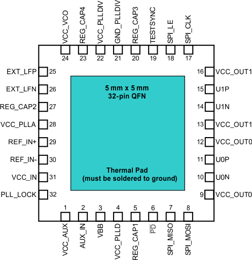
6 Pin Configuration and Functions
RHB Package
32-Pin QFN
Top View

Pin Functions
| PIN | TYPE | DESCRIPTION(1) | |
|---|---|---|---|
| NAME | NO. | ||
| AUX_IN | 2 | I | Auxiliary Input is a Crystal input pin that connect to an internal oscillator circuitry. |
| EXT_LFN | 26 | Analog | External Loop Filter Input Negative. |
| EXT_LFP | 25 | Analog | External Loop Filter Input Positive |
| GND | PAD | Ground | Ground is on Thermal PAD. See Layout Guidelines |
| GND_PLLDIV | 21 | Ground | Ground for PLL Divider circuitry. (short to GND) |
| PD | 6 | I | PD or Power-Down Pin is an active low pin and can be activated externally or through the corresponding Bit in SPI Register 2 While PD is asserted (low), the device is shut down. When PD switches high the EEPROM becomes loaded into the RAM. After the selected input clock signal becomes available, the VCO starts calibration and the PLL aims to achieve lock. All Output dividers become initiated. During self-calibration, the outputs are held static (for example, logical zero). PD pin has an internal 150-kΩ pullup resistor. Note: The SPI_LE signal has to be high in order for the EEPROM to load correctly into RAM on the Rising edge of PD. |
| PLL_LOCK | 32 | O | PLL Lock indicator |
| REF_IN+ | 29 | I | Universal Input Buffer (LVPECL, LVDS, LVCMOS) positive input for the Reference Clock. |
| REF_IN– | 30 | I | Universal Input Buffer (LVPECL, LVDS,) negative input for the Reference Clock. This pin must be pulled to ground through 1-kΩ resistor when input is selected LVCMOS. |
| REG_CAP1 | 5 | Analog | Capacitor for the internal Regulator. Connect to a 10-μF Capacitor (Y5V) |
| REG_CAP2 | 27 | Analog | Capacitor for the internal Regulator. Connect to a 10-μF Capacitor (Y5V) |
| REG_CAP3 | 20 | Analog | Capacitor for the internal Regulator. Connect to a 10-μF Capacitor (Y5V) |
| REG_CAP4 | 23 | Analog | Capacitor for the internal Regulator. Connect to a 10-μF Capacitor (Y5V) |
| SPI_CLK | 17 | I | LVCMOS input, serial Control Clock Input for the SPI bus interface, with Hysteresis. |
| SPI_LE | 18 | I | LVCMOS input, control Latch Enable for Serial Programmable Interface. Note: The SPI_LE signal has to be high in order for the EEPROM to load correctly on the Rising edge of PD. The input has an internal 150-kΩ pull-up resistor |
| SPI_MISO | 7 | O | 3-state LVCMOS Output that is enabled when SPI_LE is asserted low. It is the serial Data Output to the SPI bus interface. |
| SPI_MOSI | 8 | I | LVCMOS input, Master Out Slave In as a serial Control Data Input to CDCE62002 for the SPI bus interface. |
| TESTSYNC | 19 | I | Reserved Pin. Pull this pin down to ground using 1-kΩ resistor. |
| U0P:U0N U1P:U1N |
11,10 15,14 |
O | The outputs of CDCE62002 are user definable and can be any combination of up to 2 LVPECL outputs, 2 LVDS outputs or up to 4 LVCMOS outputs. The outputs are selectable through SPI interface. The power-up setting is EEPROM configurable. |
| VBB | 3 | Analog | Capacitor for the internal termination Voltage. Connect to a 1-μF Capacitor (Y5V) |
| VCC_AUX | 1 | A. Power | 3.3-V Supply Power for Crystal/Auxiliary Input Buffer Circuitry |
| VCC_IN | 31 | A. Power | 3.3-V Supply Power for Input Buffer Circuitry |
| VCC_OUT0 | 9, 12 | Power | 3.3-V Supply for the Output Buffers. |
| VCC_OUT1 | 13, 16 | ||
| VCC_PLLA | 28 | A. Power | 3.3-V Supply Power for the PLL circuitry. |
| VCC_PLLD | 4 | Power | 3.3-V Supply Power for the PLL circuitry. |
| VCC_PLLDIV | 22 | Power | 3.3-V Supply Power for the PLL circuitry. |
| VCC_VCO | 24 | A. Power | 3.3-V Supply Power for the VCO circuitry. |
(1) It is furthermore recommended to use a supply filter for each VCC supply domain independently. A minimum requirement is to group the supplies into four independent groups:
VCC_PLLA + VCC_VCO
VCC_PLLD + VCC_PLLDIV
VCC_IN + VCC_AUXIN
VCC_OUT0 + VCC_OUT1
All VCC pins need to be connected for the device to operate properly.
VCC_PLLA + VCC_VCO
VCC_PLLD + VCC_PLLDIV
VCC_IN + VCC_AUXIN
VCC_OUT0 + VCC_OUT1
All VCC pins need to be connected for the device to operate properly.