JAJSHR9B July 2020 – October 2021 CDCE6214-Q1
PRODUCTION DATA
- 1 特長
- 2 アプリケーション
- 3 概要
- 4 Revision History
- 5 概要 (続き)
- 6 Pin Configuration and Functions
-
7 Specifications
- 7.1 Absolute Maximum Ratings
- 7.2 ESD Ratings
- 7.3 Recommended Operating Conditions
- 7.4 Thermal Information
- 7.5 EEPROM Characteristics
- 7.6 Reference Input, Single-Ended Characteristics
- 7.7 Reference Input, Differential Characteristics
- 7.8 Reference Input, Crystal Mode Characteristics
- 7.9 General-Purpose Input Characteristics
- 7.10 Triple Level Input Characteristics
- 7.11 Logic Output Characteristics
- 7.12 Phase Locked Loop Characteristics
- 7.13 Closed-Loop Output Jitter Characteristics
- 7.14 Input and Output Isolation
- 7.15 Buffer Mode Characteristics
- 7.16 PCIe Spread Spectrum Generator
- 7.17 LVCMOS Output Characteristics
- 7.18 LP-HCSL Output Characteristics
- 7.19 LVDS Output Characteristics
- 7.20 Output Synchronization Characteristics
- 7.21 Power-On Reset Characteristics
- 7.22 I2C-Compatible Serial Interface Characteristics
- 7.23 Timing Requirements, I2C-Compatible Serial Interface
- 7.24 Power Supply Characteristics
- 7.25 Typical Characteristics
- 8 Parameter Measurement Information
- 9 Detailed Description
- 10Application and Implementation
- 11Power Supply Recommendations
- 12Layout
- 13Device and Documentation Support
- 14Mechanical, Packaging, and Orderable Information
パッケージ・オプション
デバイスごとのパッケージ図は、PDF版データシートをご参照ください。
メカニカル・データ(パッケージ|ピン)
- RGE|24
サーマルパッド・メカニカル・データ
発注情報
10.1 Application Information
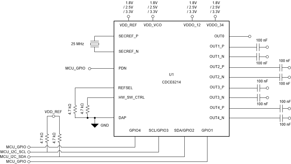
A typical application using the I2C interface and a 25-MHz crystal input is shown in Figure 10-1. The two ends of 25-MHz XTAL are connected to pin 1 and 2. The REFSEL pin is pulled down to select a secondary input. The HW_SW_CTRL can be pulled either low or high if EEPROM is used, or kept floating if EEPROM is unused. 1.8 V, 2.5 V, or 3.3 V can be supplied to the VDD_REF and VDD_VCO pins, as well as VDDO_12 and VDDO_34 pins with filtering. Data and clock lines of I2C must be pulled to VDD_REF using pullup resistors. The PDN can be connected to the MCU if a hardware reset is required, otherwise it can be left floating. The GPIO1 and 4 pins can be connected to the MCU if needed, otherwise they can be left floating. Unused outputs can be left floating.
 Figure 10-1 Typical Application Schematic With I2C Interface