JAJSHR9B July   2020  – October 2021 CDCE6214-Q1

PRODUCTION DATA  

  1. 特長
  2. アプリケーション
  3. 概要
  4. Revision History
  5. 概要 (続き)
  6. Pin Configuration and Functions
  7. Specifications
    1. 7.1  Absolute Maximum Ratings
    2. 7.2  ESD Ratings
    3. 7.3  Recommended Operating Conditions
    4. 7.4  Thermal Information
    5. 7.5  EEPROM Characteristics
    6. 7.6  Reference Input, Single-Ended Characteristics
    7. 7.7  Reference Input, Differential Characteristics
    8. 7.8  Reference Input, Crystal Mode Characteristics
    9. 7.9  General-Purpose Input Characteristics
    10. 7.10 Triple Level Input Characteristics
    11. 7.11 Logic Output Characteristics
    12. 7.12 Phase Locked Loop Characteristics
    13. 7.13 Closed-Loop Output Jitter Characteristics
    14. 7.14 Input and Output Isolation
    15. 7.15 Buffer Mode Characteristics
    16. 7.16 PCIe Spread Spectrum Generator
    17. 7.17 LVCMOS Output Characteristics
    18. 7.18 LP-HCSL Output Characteristics
    19. 7.19 LVDS Output Characteristics
    20. 7.20 Output Synchronization Characteristics
    21. 7.21 Power-On Reset Characteristics
    22. 7.22 I2C-Compatible Serial Interface Characteristics
    23. 7.23 Timing Requirements, I2C-Compatible Serial Interface
    24. 7.24 Power Supply Characteristics
    25. 7.25 Typical Characteristics
  8. Parameter Measurement Information
    1. 8.1 Reference Inputs
    2. 8.2 Outputs
    3. 8.3 Serial Interface
    4. 8.4 PSNR Test
    5. 8.5 Clock Interfacing and Termination
      1. 8.5.1 Reference Input
      2. 8.5.2 Outputs
  9. Detailed Description
    1. 9.1 Overview
    2. 9.2 Functional Block Diagram
    3. 9.3 Feature Description
      1. 9.3.1 Reference Block
        1. 9.3.1.1 Zero Delay Mode, Internal and External Path
      2. 9.3.2 Phase-Locked Loop (PLL)
        1. 9.3.2.1 PLL Configuration and Divider Settings
        2. 9.3.2.2 Spread Spectrum Clocking
        3. 9.3.2.3 Digitally-Controlled Oscillator/ Frequency Increment and Decrement - Serial Interface Mode and GPIO Mode
      3. 9.3.3 Clock Distribution
        1. 9.3.3.1 Glitchless Operation
        2. 9.3.3.2 Divider Synchronization
        3. 9.3.3.3 Global and Individual Output Enable
      4. 9.3.4 Power Supplies and Power Management
      5. 9.3.5 Control Pins
    4. 9.4 Device Functional Modes
      1. 9.4.1 Operation Modes
        1. 9.4.1.1 Fall-Back Mode
        2. 9.4.1.2 Pin Mode
        3. 9.4.1.3 Serial Interface Mode
    5. 9.5 Programming
      1. 9.5.1 I2C Serial Interface
      2. 9.5.2 EEPROM
        1. 9.5.2.1 EEPROM - Cyclic Redundancy Check
        2. 9.5.2.2 Recommended Programming Procedure
        3. 9.5.2.3 EEPROM Access
          1. 9.5.2.3.1 Register Commit Flow
          2. 9.5.2.3.2 Direct Access Flow
        4. 9.5.2.4 Register Bits to EEPROM Mapping
  10. 10Application and Implementation
    1. 10.1 Application Information
    2. 10.2 Typical Application
      1. 10.2.1 Design Requirements
      2. 10.2.2 Detailed Design Procedure
      3. 10.2.3 Application Curves
  11. 11Power Supply Recommendations
    1. 11.1 Power-Up Sequence
    2. 11.2 Decoupling
  12. 12Layout
    1. 12.1 Layout Guidelines
    2. 12.2 Layout Examples
  13. 13Device and Documentation Support
    1. 13.1 Device Support
      1. 13.1.1 Development Support
      2. 13.1.2 Device Nomenclature
    2. 13.2 Receiving Notification of Documentation Updates
    3. 13.3 サポート・リソース
    4. 13.4 Trademarks
    5. 13.5 Electrostatic Discharge Caution
    6. 13.6 Glossary
  14. 14Mechanical, Packaging, and Orderable Information

パッケージ・オプション

デバイスごとのパッケージ図は、PDF版データシートをご参照ください。

メカニカル・データ(パッケージ|ピン)
  • RGE|24
サーマルパッド・メカニカル・データ
発注情報
Direct Access Flow

In the EEPROM direct access flow, the EEPROM words are directly accessed using the address and the data bit-fields. The recommended flow is:

  1. Prepare an EEPROM image consisting of 64 words of 16 bits each.
  2. Unlock the EEPROM for write access with EE_LOCK = 0x5.
  3. Write the initial address offset to the address bit-field. Write a 0x00 to NVM_WR_ADDR.
  4. Loop through the EEPROM image from address 0 to 63 by writing each word from the image to NVM_WR_DATA. The EEPROM word address is automatically incremented by every write access to NVM_WR_DATA.
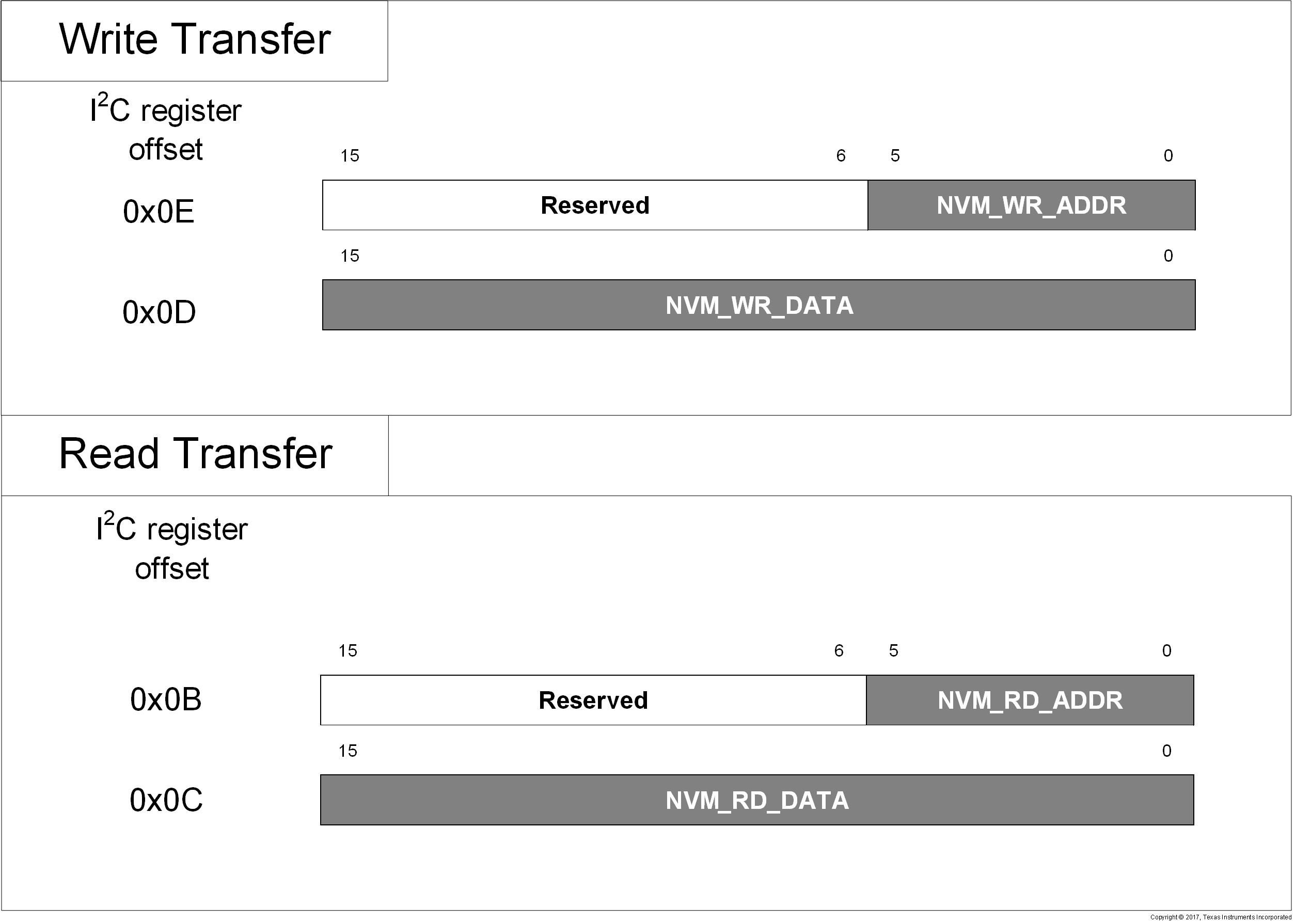
GUID-334B94FC-D9DE-4847-8DC4-350AEFD55595-low.gifFigure 9-12 EEPROM Direct Access Using I2C