JAJSDY3F July 2017 – January 2024 CDCI6214
PRODUCTION DATA
- 1
- 1 特長
- 2 アプリケーション
- 3 概要
- 4 Device Comparison
- 5 Pin Configuration and Functions
-
6 Specifications
- 6.1 Absolute Maximum Ratings
- 6.2 ESD Ratings
- 6.3 Recommended Operating Conditions
- 6.4 Thermal Information
- 6.5 EEPROM Characteristics
- 6.6 Reference Input, Single-Ended and Differential Mode Characteristics (REFP, REFN, FB_P, FB_N)
- 6.7 Reference Input, Crystal Mode Characteristics (XIN, XOUT)
- 6.8 General-Purpose Input and Output Characteristics (GPIO[4:1], SYNC/RESETN)
- 6.9 Triple Level Input Characteristics (EEPROMSEL, REFSEL)
- 6.10 Reference Mux Characteristics
- 6.11 Phase-Locked Loop Characteristics
- 6.12 Closed-Loop Output Jitter Characteristics
- 6.13 Output Mux Characteristics
- 6.14 LVCMOS Output Characteristics
- 6.15 HCSL Output Characteristics
- 6.16 LVDS DC-Coupled Output Characteristics
- 6.17 Programmable Differential AC-Coupled Output Characteristics
- 6.18 Output Skew and Delay Characteristics
- 6.19 Output Synchronization Characteristics
- 6.20 Timing Characteristics
- 6.21 I2C-Compatible Serial Interface Characteristics (SDA/GPIO2, SCL/GPIO3)
- 6.22 Timing Requirements, I2C-Compatible Serial Interface (SDA/GPIO2, SCL/GPIO3)
- 6.23 Power Supply Characteristics
- 6.24 Typical Characteristics
- 7 Parameter Measurement Information
-
8 Detailed Description
- 8.1 Overview
- 8.2 Functional Block Diagram
- 8.3 Feature Description
- 8.4 Device Functional Modes
- 8.5 Programming
- 9 Application and Implementation
- 10Register Maps
- 11Device and Documentation Support
- 12Revision History
- 13Mechanical, Packaging, and Orderable Information
パッケージ・オプション
デバイスごとのパッケージ図は、PDF版データシートをご参照ください。
メカニカル・データ(パッケージ|ピン)
- RGE|24
サーマルパッド・メカニカル・データ
発注情報
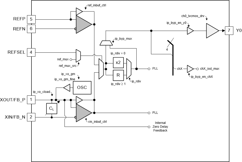
8.3.1 Reference Block
A reference clock to the PLL is fed to pins 1 (XOUT/FB_P) and 2 (XIN/FB_N) or to pins 5 (REFP) and 6 (REFN). There are multiple input stages available to adapt to many clock references. The bit-field that controls the reference input type selection is xin_inbuf_ctrl.
The reference mux selects the reference for the PLL and the PLL-bypass path. For debug purposes ip_byp_mux allows to connect the reference divider or doubler output to the clock distribution.
The buffers for the PLL-bypass path can be individually enabled and disabled using ip_byp_en_ch[4:1] and ip_byp_en_y0.
 Figure 8-2 Reference Block