JAJSDY3F July 2017 – January 2024 CDCI6214
PRODUCTION DATA
- 1
- 1 特長
- 2 アプリケーション
- 3 概要
- 4 Device Comparison
- 5 Pin Configuration and Functions
-
6 Specifications
- 6.1 Absolute Maximum Ratings
- 6.2 ESD Ratings
- 6.3 Recommended Operating Conditions
- 6.4 Thermal Information
- 6.5 EEPROM Characteristics
- 6.6 Reference Input, Single-Ended and Differential Mode Characteristics (REFP, REFN, FB_P, FB_N)
- 6.7 Reference Input, Crystal Mode Characteristics (XIN, XOUT)
- 6.8 General-Purpose Input and Output Characteristics (GPIO[4:1], SYNC/RESETN)
- 6.9 Triple Level Input Characteristics (EEPROMSEL, REFSEL)
- 6.10 Reference Mux Characteristics
- 6.11 Phase-Locked Loop Characteristics
- 6.12 Closed-Loop Output Jitter Characteristics
- 6.13 Output Mux Characteristics
- 6.14 LVCMOS Output Characteristics
- 6.15 HCSL Output Characteristics
- 6.16 LVDS DC-Coupled Output Characteristics
- 6.17 Programmable Differential AC-Coupled Output Characteristics
- 6.18 Output Skew and Delay Characteristics
- 6.19 Output Synchronization Characteristics
- 6.20 Timing Characteristics
- 6.21 I2C-Compatible Serial Interface Characteristics (SDA/GPIO2, SCL/GPIO3)
- 6.22 Timing Requirements, I2C-Compatible Serial Interface (SDA/GPIO2, SCL/GPIO3)
- 6.23 Power Supply Characteristics
- 6.24 Typical Characteristics
- 7 Parameter Measurement Information
-
8 Detailed Description
- 8.1 Overview
- 8.2 Functional Block Diagram
- 8.3 Feature Description
- 8.4 Device Functional Modes
- 8.5 Programming
- 9 Application and Implementation
- 10Register Maps
- 11Device and Documentation Support
- 12Revision History
- 13Mechanical, Packaging, and Orderable Information
パッケージ・オプション
デバイスごとのパッケージ図は、PDF版データシートをご参照ください。
メカニカル・データ(パッケージ|ピン)
- RGE|24
サーマルパッド・メカニカル・データ
発注情報
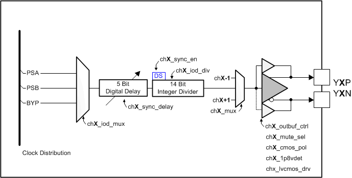
8.3.3.1 Output Channel
 Figure 8-4 Clock Distribution Pre-Scaler
Dividers
Figure 8-5 Clock Distribution, Output Channel
| INSTANCES (1) | DIVISION VALUES |
|---|---|
| PSA | 4, 5, 6 |
| PSB | 4, 5, 6 |
(1) A known phase relationship for divider synchronization with mixed division values is ensured by architecture.
Table 8-3 Output Buffer Signal Standards
| OUTPUT | LVCMOS | HCSL(2) | LVDS | AC-CML(1) | AC-LVPECL(1) |
|---|---|---|---|---|---|
| Y0 | X | ||||
| Y1 | X | X | X | X | |
| Y2 | X | X | X | X | X |
| Y3 | X | X | X | X | X |
| Y4 | x | X | x | X |
(1) The common mode shall be provided externally through an external bias source, like a voltage divider or pullup resistor. The output buffer will provide sufficient swing.
(2) For highest performance it is recommended to use HCSL on output Y1 or Y4.
Table 8-4 Output Channel Signal Selection
| NO. | INPUT SOURCE | Y1 (N=1) | Y2 (N=2) | Y3 (N=3) | Y4 (N=4) |
|---|---|---|---|---|---|
| 0 | Channel N-1 | x | x | x | |
| 1 | IOD N | x | x | x | x |
| 2 | Channel N+1 | x | x | x |
Table 8-5 Integer Divider Input Selection
| NO. | SOURCE |
|---|---|
| 0 | Pre-scaler A |
| 1 | Pre-scaler B |
| 3 | Bypass |