SLLS781D February 2007 – November 2014 CDCL1810
PRODUCTION DATA.
- 1 Features
- 2 Applications
- 3 Description
- 4 Functional Block Diagram
- 5 Revision History
- 6 Device Comparison Table
- 7 Pin Configuration and Functions
- 8 Specifications
- 9 Detailed Description
- 10Application and Implementation
- 11Power Supply Recommendations
- 12Layout
- 13Device and Documentation Support
- 14Mechanical, Packaging, and Orderable Information
10 Application and Implementation
NOTE
Information in the following applications sections is not part of the TI component specification, and TI does not warrant its accuracy or completeness. TI’s customers are responsible for determining suitability of components for their purposes. Customers should validate and test their design implementation to confirm system functionality.
10.1 Application Information
The CDCL1810 is a high-performance buffer that can generate 10 copies of CML clock outputs from a LVDS input. The programmable dividers, P0 and P1, give a high flexibility to the ratio of the output frequency to the input frequency.
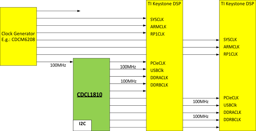
10.1.1 Clock Distribution for Multiple TI Keystone DSPs
10.1.1.1 Design Requirements
A typical application example is multi DSP chip environment. The CDCL1810 is used to buffer the common clocks to the DSP.
10.1.1.2 Detailed Design Procedure
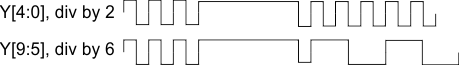
The CDCL1810 supports output group phase alignment, if a divider gets reprogrammed. The output group phase alignment circuit will disable all outputs after changing a single divider. The outputs are enabled after the phases are aligned. See Figure 9.
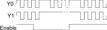
If an output gets enabled/disabled, the phase synchronization circuit will ensure that all outputs are in phase. To ensure phase alignment the outputs needs to be disabled for a short time. See Figure 10.