SLLS781D February 2007 – November 2014 CDCL1810
PRODUCTION DATA.
- 1 Features
- 2 Applications
- 3 Description
- 4 Functional Block Diagram
- 5 Revision History
- 6 Device Comparison Table
- 7 Pin Configuration and Functions
- 8 Specifications
- 9 Detailed Description
- 10Application and Implementation
- 11Power Supply Recommendations
- 12Layout
- 13Device and Documentation Support
- 14Mechanical, Packaging, and Orderable Information
8 Specifications
8.1 Absolute Maximum Ratings(1)
Over operating free-air temperature range (unless otherwise noted).| MIN | MAX | UNIT | ||
|---|---|---|---|---|
| VDD, AVDD | Supply voltage(2) | –0.3 | 2.5 | V |
| VLVDS | Voltage range at LVDS input pins(2) | –0.3 | VDD+0.6 | V |
| VI | Voltage range at all non-LVDS input pins(2) | –0.3 | VDD+0.6 | V |
(1) Stresses beyond those listed under absolute maximum ratings may cause permanent damage to the device. These are stress ratings only, and functional operation of the device at these or any other conditions beyond those indicated under recommended operating condition is not implied. Exposure to absolute-maximum-rated conditions for extended periods may affect device reliability.
(2) All voltage values are with respect to network ground terminal.
8.2 Handling Ratings
| MIN | MAX | UNIT | |||
|---|---|---|---|---|---|
| Tstg | Storage temperature range | –65 | +150 | °C | |
| V(ESD) | Electrostatic discharge | Human body model (HBM), per ANSI/ESDA/JEDEC JS-001, all pins(1) | 2000 | V | |
| Charged device model (CDM), per JEDEC specification JESD22-C101, all pins(2) | 1500 | ||||
(1) JEDEC document JEP155 states that 2000-V HBM allows safe manufacturing with a standard ESD control process.
(2) JEDEC document JEP157 states that 1500-V CDM allows safe manufacturing with a standard ESD control process.
8.3 Recommended Operating Conditions
Over operating free-air temperature range (unless otherwise noted).| MIN | NOM | MAX | UNIT | |||
|---|---|---|---|---|---|---|
| VDD | Digital supply voltage | 1.7 | 1.8 | 1.9 | V | |
| AVDD | Analog supply voltage | 1.7 | 1.8 | 1.9 | V | |
| TA | Ambient temperature (no airflow, no heatsink) | –40 | +85 | °C | ||
| TJ | Junction temperature | +105 | °C | |||
8.4 Thermal Information
| THERMAL METRIC(1) | CDCL1810 | UNIT | |
|---|---|---|---|
| RGZ Package | |||
| 48 PINS | |||
| RθJA | Junction-to-ambient thermal resistance(2) | 28.3, Airflow = 0 LFM | °C/W |
| 22.4, Airflow = 50 LFM | |||
| RθJC(top) | Junction-to-case (top) thermal resistance | 20.5 | |
| RθJC(bot) | Junction-to-case (bottom) thermal resistance | 5.3 | |
(1) For more information about traditional and new thermal metrics, see the IC Package Thermal Metrics application report, SPRA953.
(2) No heatsink; power uniformly distributed; 36 ground vias (6 x 6 array) tied to the thermal exposed pad; 4-layer high-K board.
8.5 DC Electrical Characteristics
Over recommended operating conditions (unless otherwise noted).| TEST CONDITIONS | MIN | TYP | MAX | UNIT | ||
|---|---|---|---|---|---|---|
| IVDD | Total current from digital 1.8-V supply | All outputs enabled; VDD = VDD,typ
650MHz LVDS input |
212 | mA | ||
| IAVDD | Total current from analog 1.8-V supply | All outputs enabled; AVDD = VDD,typ
650MHz LVDS input |
16 | mA | ||
| VIL,CMOS | Low level CMOS input voltage | VDD = 1.8 V | –0.2 | 0.6 | V | |
| VIH,CMOS | High level CMOS input voltage | VDD = 1.8 V | VDD –0.6 | VDD | V | |
| IIL,CMOS | Low level CMOS input current | VDD = VDD,max, VIL = 0.0 V | –120 | μA | ||
| IIH,CMOS | High level CMOS input current | VDD = VDD,max, VIH = 1.9 V | 65 | μA | ||
| VOL,SDA | Low level CMOS output voltage for the SDA pin | Sink current = 3 mA | 0 | 0.2VDD | V | |
| IOL,CMOS | Low level CMOS output current | 8 | mA | |||
8.6 AC Electrical Characteristics
Over recommended operating conditions (unless otherwise noted).8.7 AC Electrical Characteristics for The SDA/SCL Interface(1)
| PARAMETER | MIN | TYP | MAX | UNIT | |
|---|---|---|---|---|---|
| fSCL | SCL frequency | 400 | kHz | ||
| th(START) | START hold time | 0.6 | μs | ||
| tw(SCLL) | SCL low-pulse duration | 1.3 | μs | ||
| tw(SCLH) | SCL high-pulse duration | 0.6 | μs | ||
| tsu(START) | START setup time | 0.6 | μs | ||
| th(SDATA) | SDA hold time | 0 | μs | ||
| tsu(DATA) | SDA setup time | 0.6 | μs | ||
| tr(SDATA) | SCL / SDA input rise time | 0.3 | μs | ||
| tf(SDATA) | SCL / SDA input fall time | 0.3 | μs | ||
| tsu(STOP) | STOP setup time | 0.6 | μs | ||
| tBUS | bus free time | 1.3 | μs | ||
(1) See Figure 1 for the timing behavior.
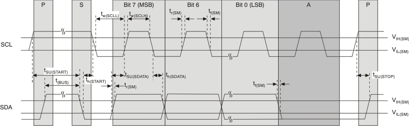 Figure 1. Timing Diagram for the SDA/SCL Serial Control Interface
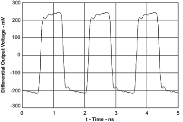
8.8 Typical Characteristics
Typical operating conditions are at VDD = 1.8V and TA = +25°C, VD,IN = 200mVPP (unless otherwise noted).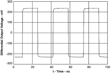
FIN = 30.72 MHz, FOUT = 30.72 MHz
FIN = 650 MHz, FOUT = 650 MHz