SCAS880F August 2009 – September 2015 CDCLVP1204
PRODUCTION DATA.
- 1 Features
- 2 Applications
- 3 Description
- 4 Revision History
- 5 Pin Configuration and Functions
-
6 Specifications
- 6.1 Absolute Maximum Ratings
- 6.2 ESD Ratings
- 6.3 Recommended Operating Conditions
- 6.4 Thermal Information
- 6.5 Terminal Characteristics
- 6.6 Electrical Characteristics: LVCMOS Input
- 6.7 Electrical Characteristics: Differential Input
- 6.8 Electrical Characteristics: LVPECL Output
- 6.9 Electrical Characteristics: LVPECL Output
- 6.10 Timing Diagrams
- 6.11 Typical Characteristics
- 7 Parameter Measurement Information
- 8 Detailed Description
- 9 Applications and Implementation
- 10Power Supply Recommendations
- 11Layout
- 12Device and Documentation Support
- 13Mechanical, Packaging, and Orderable Information
パッケージ・オプション
メカニカル・データ(パッケージ|ピン)
- RGT|16
サーマルパッド・メカニカル・データ
- RGT|16
発注情報
11 Layout
11.1 Layout Guidelines
Power consumption of the CDCLVP1204 can be high enough to require attention to thermal management. For reliability and performance reasons, the die temperature must be limited to a maximum of 125°C. That is, as an estimate, ambient temperature (TA) plus device power consumption times RθJA must not exceed 125°C.
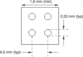
The device package has an exposed pad that provides the primary heat removal path to the printed circuit board (PCB). To maximize the heat dissipation from the package, a thermal landing pattern including multiple vias to a ground plane must be incorporated into the PCB within the footprint of the package. The exposed pad must be soldered down to ensure adequate heat conduction out of the package. Figure 24 shows a recommended land and via pattern.
11.2 Layout Example
 Figure 24. Recommended PCB Layout
11.3 Thermal Considerations
The CDCLVP1204 supports high temperatures on the printed circuit board (PCB) measured at the thermal pad. The system designer needs to ensure that the maximum junction temperature is not exceeded. Ψjb can allow the system designer to measure the board temperature with a fine gauge thermocouple and back calculate the junction temperature using Equation 1. Note that Ψjb is close to RθJB as 75 to 95% of a device's heat is dissipated by the PCB. Further information can be found at SPRA953 and SLUA566.
| Example: | ||
| Calculation of the junction-lead temperature with a 4-layer JEDEC test board using four thermal vias: | ||
| TPCB = 105°C | ||
| Ψjb = 19°C/W | ||
| PowerinclTerm = Imax × Vmax = 186 mA × 3.6 V = 669.6 mW (max power consumption including termination resistors) | ||
| PowerexclTerm = 518.6 mW (max power consumption excluding termination resistors, see SLYT127 for further details) | ||
| ΔTJunction = Ψjb × PowerexclTerm = 19°C/W × 518.6 mW = 9.85°C | ||
| TJunction = ΔTJunction + TChassis = 9.85°C + 105 °C = 114.85°C (the maximum junction temperature of 125°C is not violated) | ||