SCAS880F August 2009 – September 2015 CDCLVP1204
PRODUCTION DATA.
- 1 Features
- 2 Applications
- 3 Description
- 4 Revision History
- 5 Pin Configuration and Functions
-
6 Specifications
- 6.1 Absolute Maximum Ratings
- 6.2 ESD Ratings
- 6.3 Recommended Operating Conditions
- 6.4 Thermal Information
- 6.5 Terminal Characteristics
- 6.6 Electrical Characteristics: LVCMOS Input
- 6.7 Electrical Characteristics: Differential Input
- 6.8 Electrical Characteristics: LVPECL Output
- 6.9 Electrical Characteristics: LVPECL Output
- 6.10 Timing Diagrams
- 6.11 Typical Characteristics
- 7 Parameter Measurement Information
- 8 Detailed Description
- 9 Applications and Implementation
- 10Power Supply Recommendations
- 11Layout
- 12Device and Documentation Support
- 13Mechanical, Packaging, and Orderable Information
パッケージ・オプション
メカニカル・データ(パッケージ|ピン)
- RGT|16
サーマルパッド・メカニカル・データ
- RGT|16
発注情報
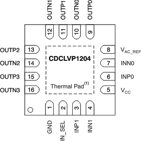
5 Pin Configuration and Functions
RGT Package
16-Pin QFN
(Top View)

1. Thermal pad must be soldered to ground.
Pin Functions
| PIN | TYPE | DESCRIPTION | |
|---|---|---|---|
| NAME | NUMBER | ||
| VCC | 5 | Power | 3.3-V supply for the device |
| GND | 1 | Ground | Device ground |
| INP0, INN0 | 6, 7 | Input | Differential input pair or single-ended input. Unused input pair can be left floating. |
| INP1, INN1 | 3, 4 | Input | Redundant differential input pair or single-ended input. Unused input pair can be left floating. |
| OUTP3, OUTN3 | 15, 16 | Output | Differential LVPECL output pair no. 3. Unused output pair can be left floating. |
| OUTP2, OUTN2 | 13, 14 | Output | Differential LVPECL output pair no. 2. Unused output pair can be left floating. |
| OUTP1, OUTN1 | 11, 12 | Output | Differential LVPECL output pair no. 1. Unused output pair can be left floating. |
| OUTP0 OUTN0 | 9, 10 | Output | Differential LVPECL output pair no. 0. Unused output pair can be left floating. |
| VAC_REF | 8 | — | Bias voltage output for capacitive-coupled inputs. Do not use VAC_REF at VCC < 3 V. If used, it is recommended to use a 0.1-μF capacitor to GND on this pin. The output current is limited to 2 mA. |
| IN_SEL | 2 | — | Pulldown (see Terminal Characteristics) MUX select input for input choice (see Table 1) |
Table 1. Input Selection Table
| IN_SEL | ACTIVE CLOCK INPUT |
|---|---|
| 0 | INP0, INN0 |
| 1 | INP1, INN1 |