SCAS886E August 2009 – December 2015 CDCLVP1212
PRODUCTION DATA.
- 1 Features
- 2 Applications
- 3 Description
- 4 Revision History
- 5 Device Comparison Table
- 6 Pin Configuration and Functions
-
7 Specifications
- 7.1 Absolute Maximum Ratings
- 7.2 ESD Ratings
- 7.3 Recommended Operating Conditions
- 7.4 Thermal Information
- 7.5 Electrical Characteristics: LVCMOS Input
- 7.6 Electrical Characteristics: Differential Input
- 7.7 Electrical Characteristics: LVPECL Output, At VCC = 2.375 V to 2.625 V
- 7.8 Electrical Characteristics: LVPECL Output, at VCC = 3.0 V to 3.6 V
- 7.9 Pin Characteristics
- 7.10 Timing Requirements
- 7.11 Typical Characteristics
- 8 Parameter Measurement Information
- 9 Detailed Description
- 10Application and Implementation
- 11Power Supply Recommendations
- 12Layout
- 13Device and Documentation Support
- 14Mechanical, Packaging, and Orderable Information
パッケージ・オプション
メカニカル・データ(パッケージ|ピン)
- RHA|40
サーマルパッド・メカニカル・データ
- RHA|40
発注情報
8 Parameter Measurement Information
8.1 Test Configurations
This section describes the function of each block for the CDCLVP1212. Figure 6 through Figure 11 illustrate how the device should be set up for a variety of test configurations.
 Figure 5. DC-Coupled LVPECL Input During Device Test
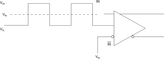
 Figure 6. DC-Coupled LVCMOS Input During Device Test
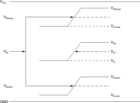
 Figure 7. Voltage Variation Over LVCMOS Vth Levels
 Figure 8. DC-Coupled LVDS Input During Device Test
 Figure 9. AC-Coupled Differential Input To Device
 Figure 10. LVPECL Output DC Configuration During Device Test
 Figure 11. LVPECL Output AC Configuration During Device Test