JAJSED0G May 2012 – January 2018 CDCM6208
PRODUCTION DATA.
- 1 特長
- 2 アプリケーション
- 3 概要
- 4 改訂履歴
- 5 Pin Configuration and Functions
-
6 Specifications
- 6.1 Absolute Maximum Ratings
- 6.2 ESD Ratings
- 6.3 Recommended Operating Conditions
- 6.4 Thermal Information, Airflow = 0 LFM
- 6.5 Thermal Information, Airflow = 150 LFM
- 6.6 Thermal Information, Airflow = 250 LFM
- 6.7 Thermal Information, Airflow = 500 LFM
- 6.8 Single-Ended Input Characteristics (SI_MODE[1:0], SDI/SDA/PIN1, SCL/PIN4, SDO/ADD0/PIN2, SCS/ADD1/PIN3, STATUS1/PIN0, RESETN/PWR, PDN, SYNCN, REF_SEL)
- 6.9 Single-Ended Input Characteristics (PRI_REF, SEC_REF)
- 6.10 Differential Input Characteristics (PRI_REF, SEC_REF)
- 6.11 Crystal Input Characteristics (SEC_REF)
- 6.12 Single-Ended Output Characteristics (STATUS1, STATUS0, SDO, SDA)
- 6.13 PLL Characteristics
- 6.14 LVCMOS Output Characteristics
- 6.15 LVPECL (High-Swing CML) Output Characteristics
- 6.16 CML Output Characteristics
- 6.17 LVDS (Low-Power CML) Output Characteristics
- 6.18 HCSL Output Characteristics
- 6.19 Output Skew and Sync to Output Propagation Delay Characteristics
- 6.20 Device Individual Block Current Consumption
- 6.21 Worst Case Current Consumption
- 6.22 Timing Requirements, I2C Timing
- 6.23 Typical Characteristics
- 7 Parameter Measurement Information
-
8 Detailed Description
- 8.1 Overview
- 8.2 Functional Block Diagram
- 8.3
Feature Description
- 8.3.1 Typical Device Jitter
- 8.3.2 Universal Input Buffer (PRI_REF, SEC_REF)
- 8.3.3 VCO Calibration
- 8.3.4 Reference Divider (R)
- 8.3.5 Input Divider (M)
- 8.3.6 Feedback Divider (N)
- 8.3.7 Prescaler Dividers (PS_A, PS_B)
- 8.3.8 Phase Frequency Detector (PFD)
- 8.3.9 Charge Pump (CP)
- 8.3.10 Fractional Output Divider Jitter Performance
- 8.3.11 Device Block-Level Description
- 8.3.12 Device Configuration Control
- 8.3.13 Configuring the RESETN Pin
- 8.3.14 Preventing False Output Frequencies in SPI/I2C Mode at Start-Up
- 8.3.15 Input MUX and Smart Input MUX
- 8.4 Device Functional Modes
- 8.5 Programming
- 8.6 Register Maps
-
9 Application and Implementation
- 9.1 Application Information
- 9.2
Typical Applications
- 9.2.1 Design Requirements
- 9.2.2
Detailed Design Procedures
- 9.2.2.1 Jitter Considerations in SERDES Systems
- 9.2.2.2 Jitter Considerations in ADC and DAC Systems
- 9.2.2.3 Configuring the PLL
- 9.2.2.4 Programmable Loop Filter
- 9.2.2.5 Loop filter Component Selection
- 9.2.2.6 Device Output Signaling
- 9.2.2.7 Integer Output Divider (IO)
- 9.2.2.8 Fractional Output Divider (FOD)
- 9.2.2.9 Output Synchronization
- 9.2.2.10 Output Mux on Y4 and Y5
- 9.2.2.11 Staggered CLK Output Power Up for Power Sequencing of a DSP
- 10Power Supply Recommendations
- 11Layout
- 12デバイスおよびドキュメントのサポート
- 13メカニカル、パッケージ、および注文情報
パッケージ・オプション
メカニカル・データ(パッケージ|ピン)
- RGZ|48
サーマルパッド・メカニカル・データ
- RGZ|48
発注情報
8.3.13 Configuring the RESETN Pin
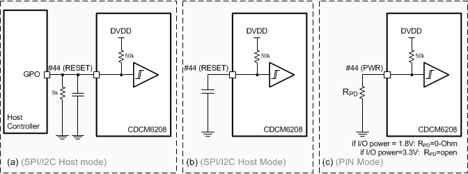
Figure 34 shows two typical applications examples of the RESETN pin and usage of the PWR pin in Pin Mode.
 Figure 34. RESETN/PWR Pin Configurations
Figure 34(a) SPI / I2C mode only: shows the RESETN pin connected to a digital device that controls device reset. The resistor and capacitor combination ensure reset is held low even if the CDCM6208 is powered up before the host controller output signal is valid.
Figure 34(b) SPI / I2C mode only: shows a configuration in which the user wishes to introduce a delay between the time that the system applies power to the device and the device exiting reset. If the user does not use a capacitor, then the device effectively ignores the state of the RESETN pin.
Figure 34(c) Pin mode only: shows a configuration useful if the device is used in Pin Mode. Here device pin number 44 becomes the PWR input. An external pull down resistor can be used to pull this pin down. If the resistor is not installed, the pin is internally pulled high.
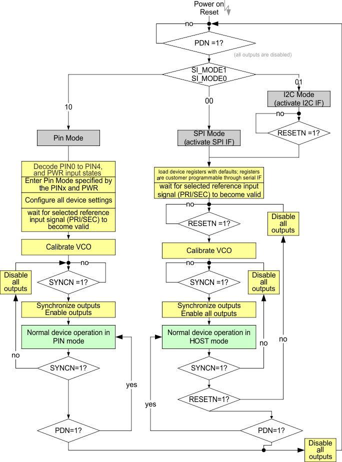
Figure 35 shows how the different possible device configurations and when the VCO becomes calibrated and the outputs turn on and off.
