SCAS943 May 2015 CDCM6208V1F
PRODUCTION DATA.
- 1 Features
- 2 Applications
- 3 Description
- 4 Simplified Schematics
- 5 Revision History
- 6 Description (continued)
- 7 Pin Configuration and Functions
-
8 Specifications
- 8.1 Absolute Maximum Ratings
- 8.2 ESD Ratings
- 8.3 Recommended Operating Conditions
- 8.4 Thermal Information, Airflow = 0 LFM
- 8.5 Thermal Information, Airflow = 150 LFM
- 8.6 Thermal Information, Airflow = 250 LFM
- 8.7 Thermal Information, Airflow = 500 LFM
- 8.8 Single Ended Input Characteristics
- 8.9 Single Ended Input Characteristics (PRI_REF, SEC_REF)
- 8.10 Differential Input Characteristics (PRI_REF, SEC_REF)
- 8.11 Crystal Input Characteristics (SEC_REF)
- 8.12 Single Ended Output Characteristics (STATUS1, STATUS0, SDO, SDA)
- 8.13 PLL Characteristics
- 8.14 LVCMOS Output Characteristics
- 8.15 LVPECL (High-Swing CML) Output Characteristics
- 8.16 CML Output Characteristics
- 8.17 LVDS (Low-Power CML) Output Characteristics
- 8.18 HCSL Output Characteristics
- 8.19 Output Skew and Sync to Output Propagation Delay Characteristics
- 8.20 Device Individual Block Current Consumption
- 8.21 Worst Case Current Consumption
- 8.22 I2C TIMING
- 8.23 SPI Timing Requirements
- 8.24 Typical Characteristics
- 9 Parameter Measurement Information
- 10Detailed Description
-
11Application and Implementation
- 11.1 Application Information
- 11.2
Typical Applications
- 11.2.1
Design Requirements
- 11.2.1.1 Device Block-level Description
- 11.2.1.2 Device Configuration Control
- 11.2.1.3 Configuring the RESETN Pin
- 11.2.1.4 Preventing False Output Frequencies in SPI/I2C Mode at Startup:
- 11.2.1.5 Power Down
- 11.2.1.6 Device Power Up Timing:
- 11.2.1.7 Input Mux and Smart Input Mux
- 11.2.1.8 Universal INPUT Buffer (PRI_REF, SEC_REF)
- 11.2.1.9 VCO Calibration
- 11.2.1.10 Reference Divider (R)
- 11.2.1.11 Input Divider (M)
- 11.2.1.12 Feedback Divider (N)
- 11.2.1.13 Prescaler Dividers (PS_A, PS_B)
- 11.2.1.14 Phase Frequency Detector (PFD)
- 11.2.1.15 Charge Pump (CP)
- 11.2.1.16
Programmable Loop Filter
- 11.2.1.16.1 Loop Filter Component Selection
- 11.2.1.16.2 Device Output Signaling
- 11.2.1.16.3 Integer Output Divider (IO)
- 11.2.1.16.4 Fractional Output Divider (FOD)
- 11.2.1.16.5 Output Synchronization
- 11.2.1.16.6 Output MUX on Y4 and Y5
- 11.2.1.16.7 Staggered CLK Output Powerup for Power Sequencing of a DSP
- 11.2.2 Detailed Design Procedure
- 11.2.3 Application Performance Plots
- 11.2.1
Design Requirements
- 12Power Supply Recommendations
- 13Layout
- 14Device and Documentation Support
- 15Mechanical, Packaging, and Orderable Information
パッケージ・オプション
メカニカル・データ(パッケージ|ピン)
- RGZ|48
サーマルパッド・メカニカル・データ
- RGZ|48
発注情報
1 Features
-
Superior Performance with Low Power:
- Low Noise Synthesizer (265 fs-rms Typical Jitter) or Low Noise Jitter Cleaner (1.6 ps-rms Typical Jitter)
- 0.5 W Typical Power Consumption
- High Channel-to-Channel Isolation and Excellent PSRR
- Device Performance Customizable Through Flexible 1.8 V, 2.5 V and 3.3 V Power Supplies, Allowing Mixed Output Voltages
- Flexible Frequency Planning:
- 4x Integer Down-divided Differential Clock Outputs Supporting LVPECL-like, CML, or LVDS-like Signaling
- 4x Fractional or Integer Divided Differential Clock Outputs Supporting HCSL, LVDS-like Signaling, or Eight CMOS Outputs
- Fractional Output Divider Achieve 0 ppm to < 1 ppm Frequency Error and Eliminates need for Crystal Oscillators and Other Clock Generators
- Output frequencies up to 800 MHz
- Two Differential Inputs, XTAL Support, Ability for Smart Switching
- SPI, I2C™, and Pin Programmable
- Professional user GUI for Quick Design Turnaround
- 7 x 7 mm 48-QFN package (RGZ)
- -40 °C to 85 °C temperature range
2 Applications
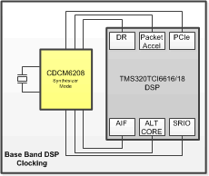
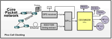
- Base Band Clocking (Wireless Infrastructure)
- Networking and Data Communications
- Keystone C66x Multicore DSP Clocking
- Storage Server, Portable Test Equipment,
- Medical Imaging, High End A/V
3 Description
The CDCM6208V1F is a highly versatile, low jitter, low-power frequency synthesizer that can generate eight low jitter clock outputs, selectable between LVPECL-like high-swing CML, normal-swing CML, LVDS-like low-power CML, HCSL, or LVCMOS, from one of two inputs that can feature a low frequency crystal or CML, LVPECL, LVDS, or LVCMOS signals for a variety of wireless infrastructure baseband, wireline data communication, computing, low power medical imaging and portable test and measurement applications. The CDCM6208V1F also features an innovative fractional divider architecture for four of its outputs that can generate any frequency with better than 1ppm frequency accuracy. The CDCM6208V1F can be easily configured through I2C or SPI programming interface and in the absence of serial interface, pin mode is also available that can set the device in 1 of 32 distinct pre-programmed configurations using control pins.
Device Information(1)
| PART NUMBER | PACKAGE | BODY SIZE (NOM) |
|---|---|---|
| CDCM6208V1F | VQFN (48) | 7.00 mm × 7.00 mm |
- For all available packages, see the orderable addendum at the end of the datasheet.
4 Simplified Schematics

