SCAS943 May 2015 CDCM6208V1F
PRODUCTION DATA.
- 1 Features
- 2 Applications
- 3 Description
- 4 Simplified Schematics
- 5 Revision History
- 6 Description (continued)
- 7 Pin Configuration and Functions
-
8 Specifications
- 8.1 Absolute Maximum Ratings
- 8.2 ESD Ratings
- 8.3 Recommended Operating Conditions
- 8.4 Thermal Information, Airflow = 0 LFM
- 8.5 Thermal Information, Airflow = 150 LFM
- 8.6 Thermal Information, Airflow = 250 LFM
- 8.7 Thermal Information, Airflow = 500 LFM
- 8.8 Single Ended Input Characteristics
- 8.9 Single Ended Input Characteristics (PRI_REF, SEC_REF)
- 8.10 Differential Input Characteristics (PRI_REF, SEC_REF)
- 8.11 Crystal Input Characteristics (SEC_REF)
- 8.12 Single Ended Output Characteristics (STATUS1, STATUS0, SDO, SDA)
- 8.13 PLL Characteristics
- 8.14 LVCMOS Output Characteristics
- 8.15 LVPECL (High-Swing CML) Output Characteristics
- 8.16 CML Output Characteristics
- 8.17 LVDS (Low-Power CML) Output Characteristics
- 8.18 HCSL Output Characteristics
- 8.19 Output Skew and Sync to Output Propagation Delay Characteristics
- 8.20 Device Individual Block Current Consumption
- 8.21 Worst Case Current Consumption
- 8.22 I2C TIMING
- 8.23 SPI Timing Requirements
- 8.24 Typical Characteristics
- 9 Parameter Measurement Information
- 10Detailed Description
-
11Application and Implementation
- 11.1 Application Information
- 11.2
Typical Applications
- 11.2.1
Design Requirements
- 11.2.1.1 Device Block-level Description
- 11.2.1.2 Device Configuration Control
- 11.2.1.3 Configuring the RESETN Pin
- 11.2.1.4 Preventing False Output Frequencies in SPI/I2C Mode at Startup:
- 11.2.1.5 Power Down
- 11.2.1.6 Device Power Up Timing:
- 11.2.1.7 Input Mux and Smart Input Mux
- 11.2.1.8 Universal INPUT Buffer (PRI_REF, SEC_REF)
- 11.2.1.9 VCO Calibration
- 11.2.1.10 Reference Divider (R)
- 11.2.1.11 Input Divider (M)
- 11.2.1.12 Feedback Divider (N)
- 11.2.1.13 Prescaler Dividers (PS_A, PS_B)
- 11.2.1.14 Phase Frequency Detector (PFD)
- 11.2.1.15 Charge Pump (CP)
- 11.2.1.16
Programmable Loop Filter
- 11.2.1.16.1 Loop Filter Component Selection
- 11.2.1.16.2 Device Output Signaling
- 11.2.1.16.3 Integer Output Divider (IO)
- 11.2.1.16.4 Fractional Output Divider (FOD)
- 11.2.1.16.5 Output Synchronization
- 11.2.1.16.6 Output MUX on Y4 and Y5
- 11.2.1.16.7 Staggered CLK Output Powerup for Power Sequencing of a DSP
- 11.2.2 Detailed Design Procedure
- 11.2.3 Application Performance Plots
- 11.2.1
Design Requirements
- 12Power Supply Recommendations
- 13Layout
- 14Device and Documentation Support
- 15Mechanical, Packaging, and Orderable Information
パッケージ・オプション
メカニカル・データ(パッケージ|ピン)
- RGZ|48
サーマルパッド・メカニカル・データ
- RGZ|48
発注情報
8 Specifications
8.1 Absolute Maximum Ratings(1)
over operating free-air temperature range (unless otherwise noted)8.2 ESD Ratings
| VALUE | UNIT | |||
|---|---|---|---|---|
| V(ESD) | Electrostatic discharge | Human body model (HBM), per ANSI/ESDA/JEDEC JS-001, all pins(1) | ±2000 | V |
| Charged device model (CDM), per JEDEC specification JESD22-C101, all pins(2) | ±500 | |||
8.3 Recommended Operating Conditions
over operating free-air temperature range (unless otherwise noted)| MIN | NOM | MAX | UNIT | |||
|---|---|---|---|---|---|---|
| VDD_Yx_Yy | Output Supply Voltage | 1.71 | 1.8/2.5/3.3 | 3.465 | V | |
| VDD_PLL1 VDD_PLL2 |
Core Analog Supply Voltage | 1.71 | 1.8/2.5/3.3 | 3.465 | V | |
| DVDD | Core Digital Supply Voltage | 1.71 | 1.8/2.5/3.3 | 3.465 | V | |
| VDD_PRI, VDD_SEC |
Reference Input Supply Voltage | 1.71 | 1.8/2.5/3.3 | 3.465 | V | |
| ΔVDD/Δt | VDD power-up ramp time (0 to 3.3 V) PDN left open, all VDD tight together PDN low-high is delayed (1) | 50 < tPDN | ms | |||
| TA | Ambient Temperature | -40 | 85 | °C | ||
| SDA and SCL in I2C MODE (SI_MODE[1:0] = 01) | ||||||
| VI | Input Voltage | DVDD = 1.8 V | –0.5 | 2.45 | V | |
| DVDD = 3.3 V | –0.5 | 3.965 | V | |||
| dR | Data Rate | 100 400 |
kbps | |||
| VIH | High-level input voltage | 0.7 x DVDD | V | |||
| VIL | Low-level input voltage | 0.3 x DVDD | V | |||
| CBUS_I2C | Total capacitive load for each bus line | 400 | pF | |||
8.4 Thermal Information, Airflow = 0 LFM(1)(2)(3)(4)
| THERMAL METRIC(1) | CDCM6208 | UNIT | |
|---|---|---|---|
| RGZ | |||
| 48 PINS VQFN | |||
| RθJA | Junction-to-ambient thermal resistance | 30.27 | °C/W |
| RθJC(top) | Junction-to-case (top) thermal resistance | 16.58 | |
| RθJB | Junction-to-board thermal resistance | 6.83 | |
| ψJT | Junction-to-top characterization parameter | 0.23 | |
| ψJB | Junction-to-board characterization parameter | 6.8 | |
| RθJC(bot) | Junction-to-case (bottom) thermal resistance | 1.06 | |
8.5 Thermal Information, Airflow = 150 LFM(1)(2)(3)(4)
| THERMAL METRIC(1) | CDCM6208 | UNIT | |
|---|---|---|---|
| RGZ | |||
| 48 PINS | |||
| RθJA | Junction-to-ambient thermal resistance | 21.8 | °C/W |
| RθJC(top) | Junction-to-case (top) thermal resistance | ||
| RθJB | Junction-to-board thermal resistance | 6.61 | |
| ψJT | Junction-to-top characterization parameter | 0.37 | |
| ψJB | Junction-to-board characterization parameter | ||
| RθJC(bot) | Junction-to-case (bottom) thermal resistance | 1.06 | |
8.6 Thermal Information, Airflow = 250 LFM(1)(2)(3)(4)
| THERMAL METRIC(1) | CDCM6208 | UNIT | |
|---|---|---|---|
| RGZ | |||
| 48 PINS | |||
| RθJA | Junction-to-ambient thermal resistance | 19.5 | °C/W |
| RθJC(top) | Junction-to-case (top) thermal resistance | ||
| RθJB | Junction-to-board thermal resistance | 6.6 | |
| ψJT | Junction-to-top characterization parameter | 0.45 | |
| ψJB | Junction-to-board characterization parameter | ||
| RθJC(bot) | Junction-to-case (bottom) thermal resistance | 1.06 | |
8.7 Thermal Information, Airflow = 500 LFM(1)(2)(3)(4)
| THERMAL METRIC(1) | CDCM6208 | UNIT | |
|---|---|---|---|
| RGZ | |||
| 48 PINS | |||
| RθJA | Junction-to-ambient thermal resistance | 17.7 | °C/W |
| RθJC(top) | Junction-to-case (top) thermal resistance | ||
| RθJB | Junction-to-board thermal resistance | 6.58 | |
| ψJT | Junction-to-top characterization parameter | 0.58 | |
| ψJB | Junction-to-board characterization parameter | ||
| RθJC(bot) | Junction-to-case (bottom) thermal resistance | 1.05 | |
8.8 Single Ended Input Characteristics
(SI_MODE[1:0], SDI/SDA/PIN1, SCL/PIN4, SDO/ADD0/PIN2, SCS/ADD1/PIN3, STATUS1/PIN0, RESETN/PWR, PDN, SYNCN, REF_SEL), DVDD = 1.71V to 1.89V, 2.375V to 2.625V, 3.135V to 3.465V, TA = –40°C to 85°C| PARAMETER | TEST CONDITIONS | MIN | TYP | MAX | UNIT | |
|---|---|---|---|---|---|---|
| VIH | Input High Voltage | 0.8 x DVDD | V | |||
| VIL | Input Low Voltage | 0.2 x DVDD | V | |||
| IIH | Input High Current | DVDD = 3.465V, VIH = 3.465 V (pull-up resistor excluded) | 30 | µA | ||
| IIL | Input Low Current | DVDD = 3.465V, VIL= 0 V | -30 | µA | ||
| ΔV/ΔT | PDN, RESETN, SYNCN, REF_SEL Input Edge Rate | 20% - 80% | 0.75 | V/ns | ||
| minPulse | PDN, RESETN, SYNCN low pulse to trigger proper device reset | 10 | ns | |||
| C IN | Input Capacitance | 2.25 | pF | |||
| RESETN, PWR, SYNCN, PDN, REF_SEL, SI_MODE[1:0]: | ||||||
| R | Input Pullup and Pulldown Resistor | 35 | 50 | 65 | kΩ | |
| SDA and SCL in I2C Mode (SI_MODE[1:0]=01) | ||||||
| VHYS_I2C | Input hysteresis | DVDD = 1.8 V | 0.1 VDVDD | V | ||
| DVDD = 2.5/3.3 V | 0.05 VDVDD | V | ||||
| IH | High-level input current | VI = DVDD | –5 | 5 | µA | |
| VOL | Output Low Voltage | IOL= 3mA | 0.2 x DVDD | V | ||
| CIN | Input Capacitance terminal | 5 | pF | |||
8.9 Single Ended Input Characteristics (PRI_REF, SEC_REF)
VDD_PRI, VDD_SEC = 1.71 V to 1.89 V, 2.375 V to 2.625 V, 3.135 V to 3.465 V, TA = –40°C to 85°C| PARAMETER | TEST CONDITIONS | MIN | TYP | MAX | UNIT | |
|---|---|---|---|---|---|---|
| fIN | Reference and Bypass Input Frequency | VDD_PRI/SEC = 1.8 V | 0.008 | 200 | MHz | |
| VDD_PRI/SEC = 3.3 V | 0.008 | 250 | MHz | |||
| VIH | Input High Voltage | 0.8 x VDD_PRI/VDD_SEC | V | |||
| VIL | Input Low Voltage | 0.2 x VDD_PRI/VDD_SEC | V | |||
| VHYST | Input hysteresis | 20 | 65 | 150 | mV | |
| IIH | Input High Current | VDD_PRI/VDD_SEC = 3.465 V, VIH = 3.465 V | 30 | µA | ||
| IIL | Input Low Current | VDD_PRI/VDD_SEC = 3.465 V, VIL = 0 V | -30 | µA | ||
| ΔV/ΔT | Reference Input Edge Rate | 20% - 80% | 0.75 | V/ns | ||
| IDC SE | Reference Input Duty Cycle | f PRI ≤ 200MHz | 40% | 60% | ||
| 200 ≤ fPRI ≤ 250 MHz | 43% | 60% | ||||
| CIN | Input Capacitance | 2.25 | pF | |||
8.10 Differential Input Characteristics (PRI_REF, SEC_REF)
VDD_PRI, VDD_SEC = 1.71 V to 1.89 V, 2.375 V to 2.625 V, 3.135 V to 3.465 V, TA = –40°C TO 85°C| PARAMETER | TEST CONDITIONS | MIN | TYP | MAX | UNIT | |
|---|---|---|---|---|---|---|
| fIN | Reference and Bypass Input Frequency | 0.008 | 250 | MHz | ||
| VI | Differential Input Voltage Swing, Peak-to-Peak | VDD_PRI/SEC = 2.5/3.3 V | 0.2 | 1.6 | VPP | |
| VDD_PRI/SEC = 1.8 V | 0.2 | 1 | VPP | |||
| VICM | Input Common Mode Voltage | CML input signaling, R4[7:6] = 00 | VDD_PRI/VDD_SEC-0.4 | VDD_PRI/VDD_SEC-0.1 | V | |
| VICM | Input Common Mode Voltage | LVDS, VDD_PRI/SEC = 1.8/2.5/3.3 V, R4[7:6] = 01, R4.1 = d.c., R4.0 = d.c. |
0.8 | 1.2 | 1.5 | V |
| VHYST | Input hysteresis | LVDS (Q4[7:6,4:3] = 01) | 15 | 65 | mVpp | |
| CML (Q4[7:6,4:3] = 00) | 20 | 85 | mVpp | |||
| IIH | Input High Current | VDD_PRI/SEC = 3.465 V, VIH = 3.465 V | 30 | µA | ||
| IIL | Input Low Current | VDD_PRI/SEC = 3.465V, VIL = 0 V | -30 | µA | ||
| ΔV/ΔT | Reference Input Edge Rate | 20% - 80% | 0.75 | V/ns | ||
| IDCDIFF | Reference Input Duty Cycle | 30% | 70% | |||
| CIN | Input Capacitance | 2.7 | pF | |||
8.11 Crystal Input Characteristics (SEC_REF)
VDD_SEC = 1.71 to 1.89 V, 2.375 V to 2.625 V, 3.135 V to 3.465 V,TA = –40°C to 85°C| PARAMETER | MIN | TYP | MAX | UNIT | |
|---|---|---|---|---|---|
| MODE OF OSCILLATION | FUNDAMENTAL | ||||
| Frequency | See note (1) | 10 | 30.72 | MHz | |
| See note (2) | 30.73 | 50 | MHz | ||
| Equivalent Series Resistance (ESR) | 10 MHz | 150(4) | Ω | ||
| 25 MHz | 70(5) | ||||
| 50 MHz | 30(6) | ||||
| On-chip load capacitance | 1.8 V / 3.3 V SEC_REFP | 3.5 | 4.5 | 5.5 | pF |
| 1.8 V SEC_REFN | 5.5 | 7.25 | 8.5 | ||
| 3.3 V SEC_REFN | 6.5 | 7.34 | 8.5 | ||
| Drive Level | See note (3) | 200 | µW | ||
8.12 Single Ended Output Characteristics (STATUS1, STATUS0, SDO, SDA)
VDD_Yx_Yy, VDD_PRI, VDD_SEC, VDD_PLLx, DVDD, VDD_VCO = 1.71V to 1.89V, 2.375V to 2.625V, 3.135V to 3.465V; TA = –40°C to 85°C (Output load capacitance 10 pF unless otherwise noted)| PARAMETER | TEST CONDITIONS | MIN | TYP | MAX | UNIT | |
|---|---|---|---|---|---|---|
| VOH | Output High Voltage | Status 1, Status 0, and SDO only; SDA is open drain and relies on external pullup for high output; IOH = 1 mA | 0.8 x DVDD | V | ||
| VOL | Output Low Voltage | IOL = 1 mA | 0.2 x DVDD | V | ||
| Vslew | Output slew rate | 30% - 70% | 0.5 | V/ns | ||
| IOZH | 3-stat Output High Current | DVDD = 3.465 V, VIH = 3.465 V | 5 | µA | ||
| IOZL | 3-stat Output Low Current | DVDD = 3.465 V, VIL = 0 V | -5 | µA | ||
| tLOS | Status Loss of Signal Detection Time | LOS_REFfvco | 1 | 2 | 1/f PFD | |
| tLOCK | Status PLL Lock Detection Time | Detect lock | 2304 | 1/f PFD | ||
| Detect unlock | 512 |
8.13 PLL Characteristics
VDD_PLLx, VDD_VCO = 1.71 V to 1.89 V, 2.375 V to 2.625 V, 3.135 V to 3.465 V, TA = –40°C TO 85°C| PARAMETER | TEST CONDITIONS | MIN | TYP | MAX | UNIT | |
|---|---|---|---|---|---|---|
| fVCO | VCO Frequency Range | 2.39 | 2.55 | GHz | ||
| KVCO | VCO Gain | 2.39 GHz | 178 | MHz/V | ||
| 2.50 GHz | 204 | |||||
| 2.55 GHz | 213 | |||||
| fPFD | PFD Input Frequency | 0.008 | 100 | MHz | ||
| ICP-L | High Impedance Mode Charge Pump Leakage | ±700 | nA | |||
| fFOM | Estimated PLL Figure of Merit (FOM) | Measured in-band phase noise at the VCO output minus 20log(N-divider) at the flat region | –224 | dBc/Hz | ||
| tSTARTUP | Startup time (see Figure 41 ) | Power supply ramp time of 1ms from 0 V to 1.7 V, final frequency accuracy of 10 ppm, fPFD = 25 MHz, CPDN_to_GND = 22nF | ||||
| w/ PRI input signal | 12.8 | ms | ||||
| w/ NDK 25 MHz crystal | 12.85 | ms |
8.14 LVCMOS Output Characteristics
VDD_Yx_Yy = 1.71 V to 1.89V, 2.375 V to 2.625 V, 3.135 V to 3.465 V, TA = –40°C TO 85°C| PARAMETER | TEST CONDITIONS | MIN | TYP | MAX | UNIT | |
|---|---|---|---|---|---|---|
| fOUT-F | Output Frequency | Fract Out divVDD_Yx_Yy = 2.5/3.3 V | 0.78 | 250 | MHz | |
| Integer out divVDD_Yx_Yy = 2.5/3.3 V | 1.55 | 250 | ||||
| Int or frac out divVDD_Yx_Yy = 1.8 V | 0.78/1.5 | 200 | ||||
| fACC-F | Output Frequency Error (1) | Fractional Output Divider | –1 | 1 | ppm | |
| VOH | Output High Voltage (normal mode) | VDD_Yx = min to max, IOH = -1 mA | 0.8 x VDD_Yx_Yy | V | ||
| VOL | Output Low Voltage(normal mode) | VDD_Yx = min to max, IOL = 100 µA | 0.2 x VDD_Yx_Yy | V | ||
| VOH | Output High Voltage (slow mode) | VDD_Yx = min to max, IOH = -100 µA | 0.7 x VDD_Yx_Yy | V | ||
| VOL | Output Low Voltage(slow mode) | VDD_Yx = min to max, IOL = 100 µA | 0.3 x VDD_Yx_Yy | V | ||
| IOH | Output High Current | V OUT = VDD_Yx_Yy/2 | ||||
| Normal mode | –50 | -8 | mA | |||
| Slow mode | –45 | -5 | mA | |||
| IOL | Output Low Current | V OUT = VDD_Yx_Yy/2 | ||||
| Normal mode | 10 | 55 | mA | |||
| Slow mode | 5 | 40 | mA | |||
| tSLEW-RATE-N | Output Rise/Fall Slew Rate (normal mode) | 20% to 80%, VDD_Yx_Yy = 2.5/3.3 V, CL = 5 pF |
5.37 | V/ns | ||
| Output Rise/Fall Slew Rate (normal mode) | 20% to 80%, VDD_Yx_Yy = 1.8 V, CL = 5 pF |
2.62 | V/ns | |||
| tSLEW-RATE-S | Output Rise/Fall Slew Rate (slow mode) | 20% to 80%, VDD_Yx_Yy = 2.5/3.3 V, CL = 5 pF |
4.17 | V/ns | ||
| Output Rise/Fall Slew Rate (slow mode) | 20% to 80%, VDD_Yx_Yy = 1.8 V, CL = 5 pF |
1.46 | V/ns | |||
| PN-floor | Phase Noise Floor | fOUT = 122.88 MHz | –159.5 | –154 | dBc/Hz | |
| ODC | Output Duty Cycle | Not in bypass mode | 45% | 55% | ||
| ROUT | Output Impedance | V OUT = VDD_Yx/2 | ||||
| Normal mode Slow mode |
30 45 |
50 74 |
90 130 |
Ω |
Note: In LVCMOS Mode, positive and negative outputs are in phase.
8.15 LVPECL (High-Swing CML) Output Characteristics
VDD_Yx_Yy = 1.71 V to 3.465 V, VDD_PRI, VDD_SEC, VDD_PLLx, DVDD, VDD_VCO = 1.71 V to 1.89 V, 2.375 V to 2.625 V, 3.135 V to 3.465 V, TA = –40°C TO 85°C| PARAMETER | TEST CONDITIONS | MIN | TYP | MAX | UNIT | ||
|---|---|---|---|---|---|---|---|
| fOUT-I | Output frequency | Integer Output Divider | 1.55 | 800 | MHz | ||
| VCM-DC | Output DC coupled common mode voltage | DC coupled with 50 Ω external termination to VDD_Yx_Yy | VDD_Yx_ Yy – 0.4 |
V | |||
| |VOD| | Differential output voltage | 100 Ω diff load AC coupling (See Figure 11), fOUT ≤ 250 MHz | |||||
| VDD_Yx_Yy ≤ 1.89 V | 0.45 | 0.75 | 1.12 | V | |||
| VDD_Yx_Yy ≥ 2.375 V | 0.6 | 0.8 | 1.12 | V | |||
| 100 Ω diff load AC coupling (See Figure 11), fOUT ≥ 250 MHz | |||||||
| VDD_Yx_Yy ≤ 1.89 V | 0.73 | V | |||||
| VDD_Yx_Yy ≥ 2.375 V | 0.55 | 0.75 | 1.12 | V | |||
| VOUT | Differential output peak-to-peak voltage | 2 x |VOD| | V | ||||
| tR/tF | Output rise/fall time | ±200 mV around crossing point | 109 | 217 | ps | ||
| 20% to 80% VOD | 211 | ps | |||||
| tslew | Output rise/fall slew rate | 3.7 | 5.1 | 7.3 | V/ns | ||
| PN-floor | Phase noise floor | VDD_Yx_Yy = 3.3 V (See Figure 53) | –161.4 | –155.8 | dBc/Hz | ||
| ODC | Output duty cycle | Not in bypass mode | 47.5% | 52.5% | |||
| ROUT | Output impedance | measured from pin to VDD_Yx_Yy | 50 | Ω | |||
8.16 CML Output Characteristics
VDD_Yx_Yy, VDD_PRI, VDD_SEC, VDD_PLLx, DVDD, VDD_VCO = 1.71V to 1.89V, 2.375V to 2.625V, 3.135V to 3.465V, TA = –40°C to 85°C| PARAMETER | TEST CONDITIONS | MIN | TYP | MAX | UNIT | ||
|---|---|---|---|---|---|---|---|
| fOUT-I | Output frequency | Integer Output Divider | 1.55 | 800 | MHz | ||
| VCM-AC | Output AC coupled common mode voltage | AC coupled with 50 Ω receiver termination | VDD_Yx_Yy – 0.46 | V | |||
| VCM-DC | Output DC coupled common mode voltage | DC coupled with 50 Ω on-chip termination to VDD_Yx_Yy |
VDD_Yx_Yy – 0.2 | V | |||
| |VOD| | Differential output voltage | 100 Ω diff load AC coupling, (See Figure 11) | 0.3 | 0.45 | 0.58 | V | |
| VOUT | Differential output peak-to-peak voltage | 2 x |VOD| | V | ||||
| tR/tF | Output rise/fall time | 20% to 80% | VDDYx = 1.8 V | 100 | 151 | 300 | ps |
| VDDYx = 2.5 V/3.3 V | 100 | 143 | 200 | ps | |||
| PN-floor | Phase noise floor at > 5 Hz offset | fOUT = 122.88 MHz | VDD_Yx_Yy = 1.8 V | –161.2 | –155.8 | dBc/Hz | |
| VDD_Yx_Yy = 3.3 V | –161.2 | –153.8 | dBc/Hz | ||||
| ODC | Output duty cycle | Not in bypass mode | 47.5% | 52.5% | |||
| ROUT | Output impedance | measured from pin to VDD_Yx_Yy | 50 | Ω | |||
8.17 LVDS (Low-Power CML) Output Characteristics
VDD_Yx_Yy, VDD_PRI, VDD_SEC, VDD_PLLx, DVDD, VDD_VCO = 1.71 V to 1.89 V, 2.375 V to 2.625 V, 3.135V to 3.465V, TA = –40°C to 85°C| PARAMETER | TEST CONDITIONS | MIN | TYP | MAX | UNIT | ||
|---|---|---|---|---|---|---|---|
| fOUT-I | Output frequency | Integer output divider | 1.55 | 400 | MHz | ||
| fOUT-F | Fractional output divider | 0.78 | 400 | MHz | |||
| fACC-F | Output frequency error (1) | Fractional output divider | -1 | 1 | ppm | ||
| VCM-AC | Output AC coupled common mode voltage | AC coupled with 50 Ω receiver termination | VDD_Yx_Yy – 0.76 | V | |||
| VCM-DC | Output DC coupled common mode voltage | DC coupled with 50 Ω on-chip termination to VDD_Yx_Yy | VDD_Yx_Yy – 0.13 | V | |||
| |VOD| | Differential output voltage | 100 Ω diff load AC coupling, (See Figure 11) | 0.247 | 0.34 | 0.454 | V | |
| VOUT | Differential output peak-to-peak voltage | 2 x |VOD| | V | ||||
| tR/tF | Output rise/fall time | ±100mV around crossing point | 300 | ps | |||
| PN-floor | Phase noise floor | fOUT= 122.88 MHz | VDD_Yx = 1.8 V | –159.3 | –154.5 | dBc/Hz | |
| VDD_Yx = 2.5/3.3 V | –159.1 | –154.9 | dBc/Hz | ||||
| ODC | Output duty cycle | Not in bypass mode | Y[3:0] | 47.5% | 52.5% | ||
| Y[7:4] | 45% | 55% | |||||
| ROUT | Output impedance | Measured from pin to VDD_Yx_Yy | 167 | Ω | |||
8.18 HCSL Output Characteristics
VDD_Yx_Yy, VDD_PRI, VDD_SEC, VDD_PLLx, DVDD, VDD_VCO = 1.71 to 1.89 V, 2.375 V to 2.625 V,3.135 V to 3.465 V, TA = –40°C to 85°C| PARAMETER | TEST CONDITIONS | MIN | TYP | MAX | UNIT | ||
|---|---|---|---|---|---|---|---|
| fOUT-I | Output frequency | Integer Output Divider | 1.55 | 400 | MHz | ||
| fOUT-F | Fractional Output Divider | 0.78 | 400 | MHz | |||
| fACC-F | Output Frequency Error (1) | Fractional Output Divider | -1 | 1 | ppm | ||
| VCM | Output Common Mode Voltage | VDD_Yx_Yy = 2.5/3.3 V | 0.2 | 0.34 | 0.55 | V | |
| VDD_Yx_Yy = 1.8 V | 0.2 | 0.33 | 0.55 | V | |||
| |VOD| | Differential Output Voltage | VDD_Yx_Yy = 2.5/3.3 V | 0.4 | 0.67 | 1.0 | V | |
| VDD_Yx_Yy = 1.8 V | 0.4 | 0.65 | 1.0 | V | |||
| VOUT | Differential Output Peak-to-peak Voltage | VDD_Yx_Yy = 2.5/3.3 V | 1.0 | 2.1 | V | ||
| VDD_Yx_Yy = 1.8 V | 2 x|VOD| | V | |||||
| tR/tF | Output Rise/Fall Time | Measured from VDIFF= –100 mV to VDIFF = +100mV, VDD_Yx_Yy = 2.5/3.3 V |
100 | 167 | 250 | ps | |
| Measured from VDIFF= –100 mV to VDIFF= +100 mV, VDD_Yx_Yy = 1.8 V |
120 | 192 | 295 | ||||
| PN-floor | Phase Noise Floor | fOUT = 122.88 MHz | VDD_Yx_Yy = 1.8 V | –158.8 | –153 | dBc/Hz | |
| VDD_Yx = 2.5/3.3 V | –157.6 | –153 | dBc/Hz | ||||
| ODC | Output Duty Cycle | Not in bypass mode | 45% | 55% | |||
8.19 Output Skew and Sync to Output Propagation Delay Characteristics
VDD_Yx_Yy = 1.71 to 1.89 V, 2.375 V to 2.625 V, 3.135V to 3.465 V, TA = –40°C to 85°C| PARAMETER | TEST CONDITIONS | MIN | TYP | MAX | UNIT | ||
|---|---|---|---|---|---|---|---|
| tPD-PS | Propagation delay SYNCN↑ to output toggling high | f VCO = 2.5 GHz | PS_A = 4 | 9 | 10.5 | 11 | 1/fPS_A |
| PS_A = 5 | 9 | 10.2 | 11 | 1/fPS_A | |||
| PS_A = 6 | 9 | 10.0 | 11 | 1/fPS_A | |||
| ΔtPD-PS | Part-to-Part Propagation delay variation SYNCN↑ to output toggling high(1) | Fixed supply voltage, temp, and device setting(1) | 0 | 1 | 1/f PS_A | ||
| OUTPUT SKEW – ALL OUTPUTS USE IDENTICAL OUTPUT SIGNALING, INTEGER DIVIDERS ONLY; PS_A = PS_B = 6, OutDiv = 4 | |||||||
| tSK,LVDS | Skew between Y[7:4] LVDS | Y[7:4] = LVDS | 40 | ps | |||
| tSK,LVDS | Skew between Y[3:0] LVDS | Y[3:0] = LVDS | 40 | ps | |||
| tSK,LVDS | Skew between Y[7:0] LVDS | Y[7:0] = LVDS | 80 | ps | |||
| tSK,CML | Skew between Y[3:0] CML | Y[3:0] = CML | 40 | ps | |||
| tSK,PECL | Skew between Y[3:0] PECL | Y[3:0] = LVPECL | 40 | ps | |||
| tSK,HCSL | Skew between Y[7:4] HCSL | Y[7:4] = HCSL | 40 | ps | |||
| tSK,SE | Skew between Y[7:4] CMOS | Y[7:4] = CMOS | 50 | ps | |||
| OUTPUT SKEW - MIXED SIGNAL OUTPUT CONFIGURATION, INTEGER DIVIDERS ONLY; PS_A = PS_B = 6, OutDiv = 4 | |||||||
| tSK,CMOS-LVDS | Skew between Y[7:4] LVDS and CMOS mixed | Y[4] = CMOS, Y[7:5] = LVDS | 2.5 | ns | |||
| tSK,CMOS-PECL | Skew between Y[7:0] CMOS and LVPECL mixed | Y[7:4] = CMOS, Y[3:0] = LVPECL | 2.5 | ns | |||
| tSK,PECL-LVDS | Skew between Y[3:0] LVPECL and LVDS mixed | Y[0] = LVPECL, Y[3:1] = LVDS | 120 | ps | |||
| tSK,PECL-CML | Skew between Y[3:0] LVPECL and CML mixed | Y[0] = LVPECL, Y[3:1] = CML | 40 | ps | |||
| tSK,LVDS-PECL | Skew between Y[7:0] LVDS and LVPECL mixed | Y[7:4] = LVDS, Y[3:0] = LVPECL | 180 | ps | |||
| tSK,LVDS-HCSL | Skew between Y[7:4] LVDS and HCSL mixed | Y[4] = LVDS, Y[7:5] = HCSL | 250 | ps | |||
| OUTPUT SKEW - USING FRACTIONAL OUTPUT DIVISION; PS_A = PS_B = 6, OutDiv = 3.125 | |||||||
| tSK,DIFF, frac | Skew between Y[7:4] LVDS using all fractional divider with the same divider setting | Y[7:4] = LVDS | 200 | ps | |||
8.20 Device Individual Block Current Consumption
VDD_Yx_Yy, VDD_PRI, VDD_SEC, VDD_PLLx, DVDD, VDD_VCO = 1.8 V, 2.5 V, or 3.3 V, TA = –40°C to 85°C, Output Types = LVPECL/CML/LVDS/LVCMOS/HCSL| BLOCK | CONDITION | TYPICAL CURRENT CONSUMPTION (mA) |
|---|---|---|
| Core | CDCM6208V1F Core, active mode, PS_A = PS_B = 4 | 75 |
| Output Buffer | CML output, AC coupled w/ 100 Ω diff load | 24.25 |
| LVPECL, AC coupled w/ 100 Ω diff load | 40 | |
| LVCMOS output, transient, 'C L' load, 'f' MHz output frequency, 'V' output swing | 1.8 + V x f OUT x (C L+ 12 x 10 -12) x 10 3 | |
| LVDS output, AC coupled w/ 100 Ω diff load | 19.7 | |
| HCSL output, 50 Ω load to GND on each output pin | 31 | |
| Output Divide Circuitry | Integer Divider Bypass (Divide = 1) | 3 |
| Integer Divide Enabled, Divide > 1 | 8 | |
| Fractional Divider Enabled | 12 | |
| additional current when PS_A differs from PS_B | 15 | |
| Total Device, CDCM6208V1F | Device Settings (V2)
|
(excl. I termination_resistors) (1.8 V: 251 mA 2.5 V: 254 mA 3.3 V: 257 mA) (incl. I termination_resistors) (1.8 V: 310 mA 2.5 V: 313 mA 3.3 V: 316 mA) |
| Total Device, CDCM6208V1F | Power Down (PDN = '0') | 0.35 |
Helpful Note: The CDCM6208V1F User GUI does an excellent job estimating the total device current consumption based on the actual device configuration. Therefore, it is recommended to use the GUI to estimate device power consumption.
The individual supply terminal current consumption for Pin mode P23 was measured to come out the following:
Table 1. Individual Supplies Measured
| Y0-1 | Y2-3 | Y4 | Y5 | Y6 | Y7 | SEC (VSEC = 1.8V) |
SEC (VSEC = 2.5V) |
PRI | PLL1 | PLL2 | VCO | DVDD | TOTAL | ||
|---|---|---|---|---|---|---|---|---|---|---|---|---|---|---|---|
| Customer EVM | PWR PIN 39 = GND VPRI = 1.8 V VOUT = 1.8 V |
61 mA | 40 mA | 21 mA | 29 mA | 30 mA | 31 mA | 12 mA | 70 mA | 1.5 mA | 295.5 mA | ||||
8.21 Worst Case Current Consumption
VDD_Yx_Yy, VDD_PRI, VDD_SEC, VDD_PLLx, DVDD, VDD_VCO = 3.45 V, TA = T-40°C to 85°C, Output Types = maximum swing, all blocks including duty cycle correction and fractional divider enabled and operating at maximum operation| BLOCK | CONDITION | CURRENT CONSUMPTION TYP / MAX |
|---|---|---|
| Total Device, CDCM6208V1F | All conditions over PVT, AC coupled outputs with all outputs terminated, device configuration: Device Settings (V2)
|
1.8 V: 310 mA / +21% (excl term) 3.3 V: 318 mA / +21% (excl term) |
8.22 I2C TIMING(2)
| PARAMETER | STANDARD MODE | FAST MODE | UNIT | |||
|---|---|---|---|---|---|---|
| MIN | MAX | MIN | MAX | |||
| fSCL | SCL Clock Frequency | 0 | 100 | 0 | 400 | kHz |
| tsu(START) | START Setup Time (SCL high before SDA low) | 4.7 | 0.6 | μs | ||
| th(START) | START Hold Time (SCL low after SDA low) | 4.0 | 0.6 | μs | ||
| tw(SCLL) | SCL Low-pulse duration | 4.7 | 1.3 | μs | ||
| tw(SCLH) | SCL High-pulse duration | 4.0 | 0.6 | μs | ||
| th(SDA) | SDA Hold Time (SDA valid after SCL low) | 0 (1) | 3.45 | 0 | 0.9 | μs |
| tsu(SDA) | SDA Setup Time | 250 | 100 | ns | ||
| tr-in | SCL / SDA input rise time | 1000 | 300 | ns | ||
| tf-in | SCL / SDA input fall time | 300 | 300 | ns | ||
| tf-out | SDA Output fall time from VIH min to VIL max with a bus capacitance from 10 pF to 400 pF | 250 | 250 | ns | ||
| tsu(STOP) | STOP Setup Time | 4.0 | 0.6 | μs | ||
| tBUS | Bus free time between a STOP and START condition | 4.7 | 1.3 | μs | ||
| tglitch_filter | Pulse width of spikes suppressed by the input glitch filter | 75 | 300 | 75 | 300 | ns |
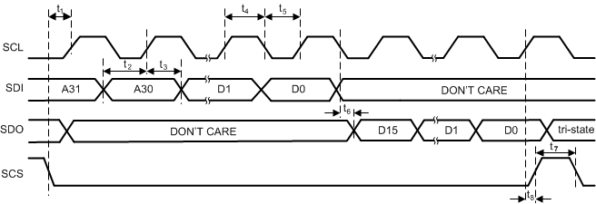 Figure 1. CDCM6208V1F SPI Port Timing
8.23 SPI Timing Requirements
| PARAMETER | MIN | NOM | MAX | UNIT | |
|---|---|---|---|---|---|
| fClock | Clock Frequency for the SCL | 20 | MHz | ||
| t1 | SPI_LE to SCL setup time | 10 | ns | ||
| t2 | SDI to SCL setup time | 10 | ns | ||
| t3 | SDO to SCL hold time | 10 | ns | ||
| t4 | SCL high duration | 25 | ns | ||
| t5 | SCL low duration | 25 | ns | ||
| t6 | SCL to SCS Setup time | 10 | ns | ||
| t7 | SCS Pulse Width | 20 | ns | ||
| t8 | SDI to SCL Data Valid (First Valid Bit after SCS) | 10 | ns | ||
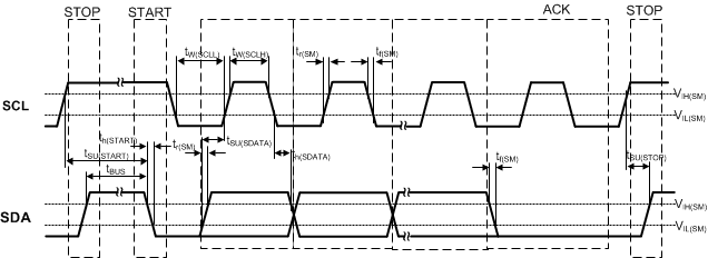 Figure 2. I2C Timing Diagram
8.24 Typical Characteristics
| fFRAC = 300 MHz |
![CDCM6208V1F PSRR (in dBc and DJ
[ps]) Over Frequency [Hz] and Output Signal Format CDCM6208V1F PSRR_in_dBc_and_DJ_ps_SCAS931.gif](/ods/images/SCAS943/PSRR_in_dBc_and_DJ_ps_SCAS931.gif)
| f OUT = 122 MHz |
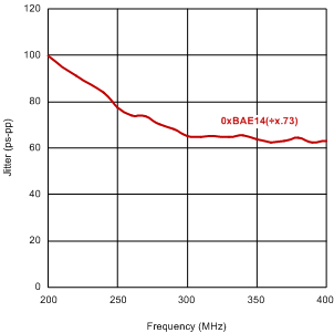
| Using Divide by x.73 Example |
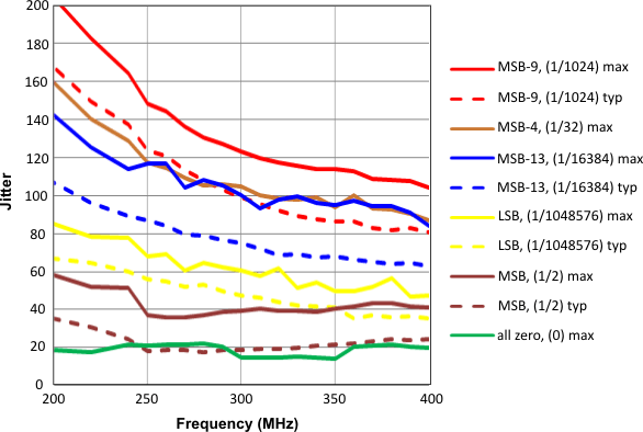
(Maximum Jitter Across Process, Voltage & Temperature)
8.24.1 Fractional Output Divider Jitter Performance
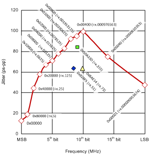
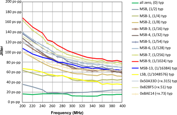
The fractional output divider jitter performance is a function of the fraction output divider input frequency as well as actual fractional divide setting itself. To minimize the fractional output jitter, it is recommended to use the least number of fractional bits and the highest input frequency possible into the divider. As observable in Figure 3, the largest jitter contribution occurs when only one fractional divider bit is selected, and especially when the bits in the middle range of the fractional divider are selected. Tested using a LeCroy 40 Gbps RealTime scope over a time window of 200 ms. The RJ impact on TJ is estimated for a BERT 10(–12) – 1. This measurement result is overly pessimistic, as it does not bandwidth limit the high-frequencies. In a real system, the SERDES TX will BW limit the jitter through its PLL roll-off above the TX PLL bandwidth of typically bit rate divided by 10.
8.24.2 Power Supply Ripple Rejection (PSRR) versus Ripple Frequency
See Figure 7 for reference.
Many system designs become increasingly more sensitive to power supply noise rejection. In order to simplify design and cost, the CDCM6208V1F has built in internal voltage regulation, improving the power supply noise rejection over designs with no regulators. As a result, the following output rejection is achieved:
The DJ due to PSRR can be estimated using Equation 1:

Example:Therefore, if 100 mV noise with a frequency of 10 kHz were observed at the output supply, the according output jitter for a 122.88 MHz output signal with LVDS signaling could be estimated with DJ = 0.7ps.