SCAS643I September   2000  – October  2017 CDCV304

PRODUCTION DATA.  
  1. 1Features
  2. 2Description
  3. 3Revision History
  4. 4Pin Configuration and Functions
  5. 5Specifications
    1. 5.1 Absolute Maximum Ratings
    2. 5.2 Recommended Operating Conditions
    3. 5.3 Thermal Information
    4. 5.4 Electrical Characteristics
    5. 5.5 Timing Requirements
    6. 5.6 Switching Characteristics: VDD = 2.5 V ± 10%
    7. 5.7 Switching Characteristics: VDD = 3.3 V ± 10%
    8. 5.8 Typical Characteristics
  6. 6Parameter Measurement Information
  7. 7Detailed Description
    1. 7.1 Functional Block Diagram
    2. 7.2 Device Functional Modes
  8. 8Device and Documentation Support
    1. 8.1 Receiving Notification of Documentation Updates
    2. 8.2 Community Resources
    3. 8.3 Trademarks
    4. 8.4 Electrostatic Discharge Caution
    5. 8.5 Glossary
  9. 9Mechanical, Packaging, and Orderable Information

パッケージ・オプション

メカニカル・データ(パッケージ|ピン)
サーマルパッド・メカニカル・データ
発注情報

Detailed Description

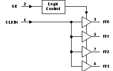
Functional Block Diagram

CDCV304 fbd_cas643.gif

Device Functional Modes

Table 1. Function Table

INPUTS OUTPUTS
CLKIN OE 1Y[0:3]
L L L
H L L
L H L
H H H