SCAS643I September 2000 – October 2017 CDCV304
PRODUCTION DATA.
5 Specifications
5.1 Absolute Maximum Ratings
over operating free-air temperature range (unless otherwise noted) (1)| MIN | MAX | UNIT | |
|---|---|---|---|
| Supply voltage range, VDD | –0.5 | 4.3 | V |
| Input voltage range, VI (2) (3) | –0.5 | VDD + 0.5 | V |
| Output voltage range, VO (2) (3) | –0.5 | VDD + 0.5 | V |
| Input clamp current, IIK (VI < 0 or VI> VDD) | –50 | 50 | mA |
| Output clamp current, IOK (VO < 0 or VO > VDD) | –50 | 50 | mA |
| Continuous total output current, IO (VO = 0 to VDD) | –50 | 50 | mA |
| Package thermal impedance, θJA: PW package | 230.5 | °C/W | |
| Junction temperature, Tj, max | 125 | °C | |
| Storage temperature range Tstg | –65 | 150 | °C |
(1) Stresses beyond those listed under Absolute Maximum Ratings may cause permanent damage to the device. These are stress ratings only, which do not imply functional operation of the device at these or any other conditions beyond those indicated under Recommended Operating Conditions. Exposure to absolute-maximum-rated conditions for extended periods may affect device reliability.
(2) The input and output negative voltage ratings may be exceeded if the input and output clamp-current ratings are observed.
(3) This value is limited to 4.6 V maximum.
5.2 Recommended Operating Conditions
5.3 Thermal Information
| THERMAL METRIC(1) | THERMAL AIR FLOW (CFM) | CDCV304 | UNIT | ||
|---|---|---|---|---|---|
| PW (TSSOP) | |||||
| 8 PINS | |||||
| RθJA | Junction-to-ambient thermal resistance | High K | 0 | 149 | °C/W |
| 150 | 142 | ||||
| 250 | 138 | ||||
| 500 | 132 | ||||
| Low K | 230 | ||||
| 185 | |||||
| 170 | |||||
| 150 | |||||
| RθJC(top) | Junction-to-case (top) thermal resistance | 43.7 | |||
| RθJB | Junction-to-board thermal resistance | 102 | |||
| ψJT | Junction-to-top characterization parameter | 1.8 | |||
| ψJB | Junction-to-board characterization parameter | 100.2 | |||
(1) For more information about traditional and new thermal metrics, see the Semiconductor and IC Package Thermal Metrics application report.
5.4 Electrical Characteristics
over recommended operating free-air temperature range (unless otherwise noted)| PARAMETER | TEST CONDITIONS | MIN | TYP(1) | MAX | UNIT | ||
|---|---|---|---|---|---|---|---|
| VIK | Input voltage | VDD = 3 V, | II = –18 mA | –1.2 | V | ||
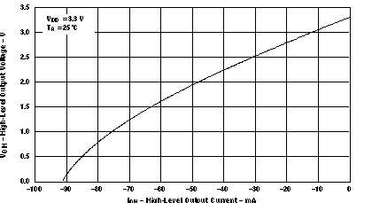
| VOH | High-level output voltage | VDD = 2.3 V, | IOH = –8 mA | 1.8 | V | ||
| VDD = 2.3 V, | IOH = –16 mA | 1.5 | |||||
| VDD = min to max, | IOH = –1 mA | VDD – 0.2 | |||||
| VDD = 3 V, | IOH = –24 mA | 2 | |||||
| VDD = 3 V, | IOH = –12 mA | 2.4 | |||||
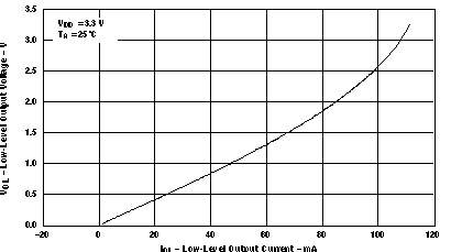
| VOL | Low-level output voltage | VDD = 2.3 V, | IOL = 8 mA | 0.5 | V | ||
| VDD = 2.3 V, | IOL = 16 mA | 0.7 | |||||
| VDD = min to max, | IOL = 1 mA | 0.2 | |||||
| VDD = 3 V, | IOL = 24 mA | 0.8 | |||||
| VDD = 3 V, | IOL = 12 mA | 0.55 | |||||
| IOH | High-level output current | VDD = 3 V, | VO = 1 V | –50 | mA | ||
| VDD = 3.3 V, | VO = 1.65 V | –55 | |||||
| IOL | Low-level output current | VDD = 3 V, | VO = 2 V | 60 | mA | ||
| VDD = 3.3 V, | VO = 1.65 V | 70 | |||||
| II | Input current | VI = VO or VDD | ±5 | μA | |||
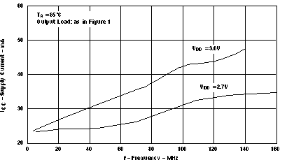
| IDD | Dynamic current, see Figure 1 | f = 67 MHz, | VDD = 2.7 V | 28 | mA | ||
| f = 67 MHz, | VDD = 3.6 V | 37 | |||||
| CI | Input capacitance | VDD = 3.3 V, | VI = 0 V or VDD | 3 | pF | ||
| CO | Output capacitance | VDD = 3.3 V, | VI = 0 V or VDD | 3.2 | pF | ||
(1) All typical values are with respect to nominal VDD and TA = 25°C.
5.5 Timing Requirements
over operating free-air temperature range (unless otherwise noted)| PARAMETER | TEST CONDITIONS | MIN | TYP | MAX | UNIT | |
|---|---|---|---|---|---|---|
| fclk | Clock frequency | 0 | 200 | MHz | ||
5.6 Switching Characteristics: VDD = 2.5 V ± 10%
VDD = 2.5 V ± 10%, CL= 10 pF (unless otherwise noted)| PARAMETER | TEST CONDITIONS | MIN | TYP(1) | MAX | UNIT | |
|---|---|---|---|---|---|---|
| tPLH | Low-to-high propagation delay | See Figure 4 and Figure 5 | 2 | 2.9 | 4.5 | ns |
| tPHL | High-to-low propagation delay | 2 | 3 | 4.5 | ||
| tsk(o) | Output skew(2) | See Figure 6 | 50 | 150 | ps | |
| tr | Output rise slew rate | 1.5 | 2.2 | 4 | V/ns | |
| tf | Output fall slew rate | 1.5 | 2.2 | 4 | V/ns | |
(1) All typical values are with respect to nominal VDD.
(2) The tsk(o) specification is only valid for equal loading of all outputs.
5.7 Switching Characteristics: VDD = 3.3 V ± 10%
VDD = 3.3 V ± 10%, CL= 10 pF (unless otherwise noted)| PARAMETER | TEST CONDITIONS | MIN | TYP(1) | MAX | UNIT | |
|---|---|---|---|---|---|---|
| tPLH | Low-to-high propagation delay | See Figure 4 and Figure 5 | 1.8 | 2.4 | 3 | ns |
| tPHL | High-to-low propagation delay | 1.8 | 2.5 | 3 | ||
| tsk(o) | Output skew(3) | 50 | 100 | ps | ||
| tjitter | Additive phase jitter from input to output 1Y0 | 12 kHz to 5 MHz, fout = 30.72 MHz | 63 | fs rms | ||
| 12 kHz to 20 MHz, fout = 125 MHz | 56 | |||||
| tsk(p) | Pulse skew | VIH = VDD, VIL = 0 V | 150 | ps | ||
| tsk(pr) | Process skew | 0.2 | 0.3 | ns | ||
| tsk(pp) | Part-to-part skew | 0.25 | 0.4 | ns | ||
| thigh | Clock high time, see Figure 7 | 66 MHz | 6 | ns | ||
| 140 MHz | 3 | |||||
| tlow | Clock low time, see Figure 7 | 66 MHz | 6 | ns | ||
| 140 MHz | 3 | |||||
| tr | Output rise slew rate(2) | VO = 0.4 V to 2 V | 1.5 | 2.7 | 4 | V/ns |
| tf | Output fall slew rate(2) | VO = 2 V to 0.4 V | 1.5 | 2.7 | 4 | V/ns |
(1) All typical values are with respect to nominal VDD.
(2) This symbol is according to PCI-X terminology.
(3) The tsk(o) specification is only valid for equal loading of all outputs.


